Continue to Site

Welcome to EDAboard.com

Welcome to our site! EDAboard.com is an international Electronics Discussion Forum focused on EDA software, circuits, schematics, books, theory, papers, asic, pld, 8051, DSP, Network, RF, Analog Design, PCB, Service Manuals... and a whole lot more! To participate you need to register. Registration is free. Click here to register now.

If anybody need help in EAGLE, ask me in this POST !

Status
Not open for further replies.
Hi, I have a question about Eagle software.

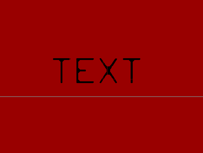
I want to write text in a board, but I don't want to write with the metal (or tracks), I want the opposite. That is, I want to clean the metal were the characters will be, and the text will be readable because it has metalization around. Was I clear about what I want?

I think I have to put the text in some layer, but I don't know in which I should put it.

Thanks
 

One way is to fill the area with copper using polygon fill then write the text in the tRestrict layer - layer 41.

Keith
 

Thanks for the quick reply.

Unfortunately that doesn't work. When I do that, and then click on Ratsnest, the text appears writen with copper, and around the text the copper is cleared, and I want the opposite, maintain the copper around the text and clear the copper to form the letters.
 

Strange, that works for me, assuming this is what you want:


Keith.

Are you sure your wrote the text in layer 41?
 

That is exactly what I want...

I am doing that this way:
- Limit the area with the polygon tool, then click on Ratsnest (the area is then filled with copper)
- Choose the 41tRestrict layer, choose the text tool, write what I want and then place it in the area where I drawn the polygon (the text appears in a lighter red compared to the red of top layer)
- Then click on Ratsnest and the copper around the text is cleared, while the text stays red (now with the same red as the top layer)
 

Maybe you could upload your file and I will have a look. Top restrict should prevent copper in the top layer.

Keith.
 

I uploaded the *.brd file.

I want to write IN near the left SMA connector and OUT near the right SMA connector, and fill the rest with copper.
 

Attachments

  • if_filter.zip
    3.3 KB · Views: 60

OK, I see the problem. You have used a rectangle rather than "polygon fill". Rectangles are of limited use - they are always solid. Delete your rectangles and replace them with polygon fills. It will then work.

Keith.
 

I want to right the text on the upper side, not were I draw the rectangles. Anyway, I cleared the rectangles, design a polygon all around the board, write the text in the 41tRestrict layer, then click on Ratsnest and... same thing happen. The text is writen with copper while copper is cleared around the text.

Maybe it has something to do with the polygon options?
 

Here is what I did with your file.

Keith.
 

Attachments

  • if_filterKR.zip
    3.3 KB · Views: 8,706

Hum... maybe it's something with Eagle options, because this is how your file appears here:
**broken link removed**

If I click in the Ratsnest icon, Eagle will fill the polygon with copper except around the text, while the letters are written with copper.

What I wanted was something like this, but with the text written without copper:
**broken link removed**
 

You need to "ratsnest" it first. Also, I assume you have the option "ratsnest processes polygons" set? This is what it looks like after ratsnesting:


Keith.
 

this is what you want I think, along with an image of what it looks like on my computer.

Keith.
 

Attachments

  • if_filterKR2.zip
    52.8 KB · Views: 65

This is what happens when I open the last file you sent (if_filterkr2.brd):

First, I get a warning (don't know if this is relevant):
**broken link removed**

Then I click OK and this is what the board looks like:
**broken link removed**

Then I click on Ratsnest and this is the result:
**broken link removed**

EDIT: I forgot something... The text is still there, in the 41tRestrict. But when I took this PtrScr I didn't have that layer visible.

Sorry I'm giving you so much trouble... I'll just print the board with the text written with copper.

Thanks for your help and patience! :p
 

Could you send me your board & schematic file? Also, when opening my file, close all other files first (in particular your schematic). The error message is simply because the schematic & board have different file names - there is no schematic to match the board file I sent.

Keith.

---------- Post added at 17:33 ---------- Previous post was at 17:30 ----------

I think I have found it. Under "options" | "user interface" , set "always vector font". Then ratsnest again.

Keith.
 
OMG, that's it! Ahh, I knew it had to be some option turned on/off.

Thank you very much! :)
 

i need to do 3d board modelling, can eagle do this?
 

ada yg tau untuk cari RS 232 atau DB9 9pin d library eagle 5.4?

---------- Post added at 19:41 ---------- Previous post was at 19:39 ----------

can't find DB9 port for serial module schematic in eagle 5.4?
 

Status
Not open for further replies.

Part and Inventory Search

Welcome to EDABoard.com

Sponsor

Back
Top