akbarza
Full Member level 2
hi
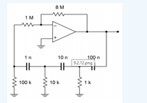
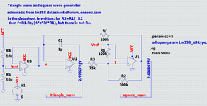
I found the below schematic in an Lm358 datasheet that belongs to www.onsemi.com.
by attention to the pic, in the datasheet is written that for R3=R1||R2 then the oscillation frequency is f=R1*Rc/(4*c*Rf*R1). but there is no Rc in the schematic.
1)how can analyze the circuit to obtain a formula for frequency?
2)can explain to me why in node triangle_wave, the shape of oscillation is a triangle wave, and also for node square_wave?
3) as we know this circuit will be connected to another circuit and it causes a load effect. How can I import the role of load in the schematic?
4)suppose the design is for a special frequency and R's and c are determined for that frequency. is there any condition on Opamp as Unity gain bandwidth or others that Opamp must satisfy?
thanks
") from staying up so late the nite before.
from staying up so late the nite before.