Continue to Site

Welcome to EDAboard.com

Welcome to our site! EDAboard.com is an international Electronics Discussion Forum focused on EDA software, circuits, schematics, books, theory, papers, asic, pld, 8051, DSP, Network, RF, Analog Design, PCB, Service Manuals... and a whole lot more! To participate you need to register. Registration is free. Click here to register now.

analyze and find oscillating frequency

akbarza

Full Member level 2
Joined
Dec 18, 2013
Messages
131
Helped
0
Reputation
0
Reaction score
0
Trophy points
1,296
Activity points
2,556
hi
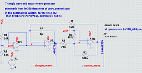
I found the below schematic in an Lm358 datasheet that belongs to www.onsemi.com.
by attention to the pic, in the datasheet is written that for R3=R1||R2 then the oscillation frequency is f=R1*Rc/(4*c*Rf*R1). but there is no Rc in the schematic.
1)how can analyze the circuit to obtain a formula for frequency?
2)can explain to me why in node triangle_wave, the shape of oscillation is a triangle wave, and also for node square_wave?
3) as we know this circuit will be connected to another circuit and it causes a load effect. How can I import the role of load in the schematic?
4)suppose the design is for a special frequency and R's and c are determined for that frequency. is there any condition on Opamp as Unity gain bandwidth or others that Opamp must satisfy?
thanks
 

Attachments

  • triangle_generator.png
    triangle_generator.png
    49.2 KB · Views: 89
Hi,

here you are not missing a resistor with designator Rc, it shoud be the product of R times C (R • C). The picture below is form an MOTOROLA datasheet [1]. In gerneral, if your are in doubt of a equations in a datasheet which is quite obviously corrupted be converting it, have a look if this IC is manufactured by someone else. And here, try to find a datasheet from a retired manufacturer.

LM358_Motorola.png


[1] https://pdf1.alldatasheet.com/datasheet-pdf/view/3067/MOTOROLA/LM358.html

BR
--- Updated ---

.... sorry it just realized I have reffered to the wrong design.

SORRY!
 
First of all, sorry for the wrong initial replay!

I had a second look on the circuitry, also by means of a simulation. By comparing the simulation result and the given equation, you will end up with R2 being your Rc you are looking for.

If you are checking this with your simulation, increase VCC as the input common mode voltage cause some troubles otherwise as it's upper limit is stated with "The upper end of the common mode voltage range is VCC − 1.7 V".

BR
 
  1. LM358 are hard to work with only 5V, due to 2V headroom.
  2. Drop Vref to 2V to reduce Vin range.
  3. Move R1 from Vref to 0V ( it was in the wrong place) and raise value to optimize duty cycle. to 50%
If Vref is reduced below Vcc/2 then so too must the triangle wave feedback.

Any questions?
Calculate from Vol to Voh swing to get Vthevenin average = Vref or start with my guestimate of 180k

Always read the datasheet fully to understand Vin.cm and Vo range.

With R1= 330 k , you may get near 50% df and 10 Hz

Next time only use CMOS RRIO for these designs.
 
Last edited:
  1. Your biggest error was R1 to Vref which altered Vref into a non-triangle wave. Use buffered Vref. or gnd as I said.
  2. Next choose lower R from Triangle (Integrator) out which integrates around Vref and a bigger R from Square wave feedback to Vin+ feedback, which changes hysteresis and f but reduces error from non-rail-to-rail SQR out.
  3. So swap R2<>R3. Now R1 may not help or is needed as much , so R1 to ground is near 390k for 50% d.f. and just below 10 Hz
--- Updated ---

A rough look :

View attachment 187375


Regards, Dana.
I'm surprised to see Simetrix put Vcc and Vee on the wrong side
 
  1. Your biggest error was R1 to Vref which altered Vref into a non-triangle wave. Use buffered Vref. or gnd as I said.
  2. Next choose lower R from Triangle (Integrator) out which integrates around Vref and a bigger R from Square wave feedback to Vin+ feedback, which changes hysteresis and f but reduces error from non-rail-to-rail SQR out.
  3. So swap R2<>R3. Now R1 may not help or is needed as much , so R1 to ground is near 390k for 50% d.f. and just below 10 Hz
--- Updated ---


I'm surprised to see Simetrix put Vcc and Vee on the wrong side
I flipped the symbol.

Regards, Dana.
 
My simulators only swap inputs not the whole symbol.
But I am also surprised you also swapped R2, R3 but never mentioned it.
I did not keep the same naming, should have. Just used the orig circuit
( minus same component names ) and dropped the redundant.

Duty cycle controlled by Vref value, V2.


Regards, Dana.
 
Both OPs are operated at Vcm = Vref, thus Vref= Vcc/2 can work. Problem is however LM358 asymmetric output swing, can be fixed by a low kOhm pull-up resistor at OP output enforcing class A operation, presuming you don't have a recent rail-to-rail OP at hand.
 
Hi,

Your biggest error was R1 to Vref which altered Vref into a non-triangle wave. Use buffered Vref. or gnd as I said.

there is no error at all. The initial question was how the below circuitry recommended in the datasheet of the LM358 works and how to determine its frequency. Reply #4 address the equation in question. Further, the Vcm problem at Vcc = 5V, if using a bipolar opamp was mentioned there as well.

Screenshot_20231229-104608~2.png
 
Hi,


there is no error at all. The initial question was how the below circuitry recommended in the datasheet of the LM358 works and how to determine its frequency. Reply #4 address the equation in question. Further, the Vcm problem at Vcc = 5V, if using a bipolar opamp was mentioned there as well.

View attachment 187381
please read again. The label is not buffered, but the optimal bias was not discussed with criteria for mixed feedback amplitude. Reducing Square feedback also helped this but reduced Triangle output at same time
1703847367598.png
 
Hi,

yes, but R1 has to be connected to Vref as shown in the application schematic. But I agree of course the reference voltage has to be buffered.

BR
 
no the label has to be moved in the simulation and R1 doesn't help to reduced Vref at Vcc=5V, in fact the integrator reference must be tweaked due to SW asymmetrical saturation. Maybe it's sufficient for Vcc=15
 
Last edited:
Adding 1k ohm pullups did not seem to affect sim done in post #8. Odd the Voh seemed unaffected.

1703852046022.png


Trimming Vref will reach 50% duty cycle. Note I changed OpAmp to LM324 to see
if that affected results, did not. Note adding pullups did not change output of
comparator, Vol, so I am suspicious the models are over simplified. So I changed
the 1K PUs to 100 ohms and everything was affected, including duty cycle. But
100 ohms takes part out of spec for output ratings.


Regards, Dana.
 
Last edited:
Looks like R1 has no actual purpose. Also Vref buffer can be omitted if voltage divider is sufficient low impedance.

Vref set to 1.9 V for about symmetrical output with Onsemi transistor level SPICE model. Other models have different output characteristic.

1703854862704.png

--- Updated ---

I noticed that pull-up resistor doesn't have the expected effect according to datasheet output characteristic with some models. Too low pull-up will also increase low saturation voltage. I omitted pull-up to reduce complexity.
 

Attachments

  • triangle.zip
    6.7 KB · Views: 55

LaTeX Commands Quick-Menu:

Part and Inventory Search

Welcome to EDABoard.com

Sponsor

Back
Top