dick_freebird
Advanced Member level 7
Re: Top level IO cells connection ( multiple IO voltages and global source use ) and
I have had the pleasure of working for decade in a technology
where the PDK never modeled the GGNMOS clamp's breakdown
action at all, and insisted the GGNMOS clamp PCell was righteous
and inviolable.
Yet ESD results were always very poor.
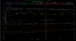
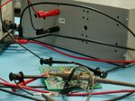
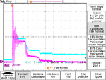
I had to build my own TLP rig and take my own clamp response
data and fit my own ESD clamp model (trivial really, add a zener
and a resistor to fit bench data in the GGNMOS subcircuit layer
of the modeling hierarchy.
If you have this then you can -design- ESD protection rather
than playing with LEGOs and the set's missing a piece. I'm
talking full pin-pin simulations showing pin I, V to criticize
against what the schematics say is attached.
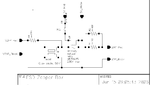
I made "stinger" macros parameterized such that parametric
analysis nested loops (of pin# indices) can perform the
pin-pin combo zapping and show a "worst case envelope"
when plotted. Loop pinX, pinY and zapPolarity and go have
lunch and a nap.


An actual adjunct breakdown model:
Kill all the forward params and tweak the reverse breakdown to fit
bench waveforms from TLP
simulator lang=spice
******************************************************************
* Clamp breakdown model with series resistance*
* area normalized to w=1um at area=1 *
******************************************************************
.model dzGGNMOS Diode
+Level = 1
+IS =1E-99
+ISW =0.00
+N =99
+NS =1.0
+IMAX =1.0
+RS =1400
+RSW =0.00
+BV =4.7
+IBV =1.00E-05
+NZ =6.0
+TRS =3.47E-03
+CTA =0.00
+CTP =0.00
+EG =99.9
+XTI =9.8056
+Cjo =1E-18
+Mj =0.0627
+Pb =0.173
+Cjsw= 0
+Mjsw= 0.33
+vjsw= 0.7
+Pta= 0
+Ptp= 0
***********************************************************
I have had the pleasure of working for decade in a technology
where the PDK never modeled the GGNMOS clamp's breakdown
action at all, and insisted the GGNMOS clamp PCell was righteous
and inviolable.
Yet ESD results were always very poor.
I had to build my own TLP rig and take my own clamp response
data and fit my own ESD clamp model (trivial really, add a zener
and a resistor to fit bench data in the GGNMOS subcircuit layer
of the modeling hierarchy.
If you have this then you can -design- ESD protection rather
than playing with LEGOs and the set's missing a piece. I'm
talking full pin-pin simulations showing pin I, V to criticize
against what the schematics say is attached.
I made "stinger" macros parameterized such that parametric
analysis nested loops (of pin# indices) can perform the
pin-pin combo zapping and show a "worst case envelope"
when plotted. Loop pinX, pinY and zapPolarity and go have
lunch and a nap.
An actual adjunct breakdown model:
Kill all the forward params and tweak the reverse breakdown to fit
bench waveforms from TLP
simulator lang=spice
******************************************************************
* Clamp breakdown model with series resistance*
* area normalized to w=1um at area=1 *
******************************************************************
.model dzGGNMOS Diode
+Level = 1
+IS =1E-99
+ISW =0.00
+N =99
+NS =1.0
+IMAX =1.0
+RS =1400
+RSW =0.00
+BV =4.7
+IBV =1.00E-05
+NZ =6.0
+TRS =3.47E-03
+CTA =0.00
+CTP =0.00
+EG =99.9
+XTI =9.8056
+Cjo =1E-18
+Mj =0.0627
+Pb =0.173
+Cjsw= 0
+Mjsw= 0.33
+vjsw= 0.7
+Pta= 0
+Ptp= 0
***********************************************************
Attachments
Last edited: