Continue to Site

Welcome to EDAboard.com

Welcome to our site! EDAboard.com is an international Electronics Discussion Forum focused on EDA software, circuits, schematics, books, theory, papers, asic, pld, 8051, DSP, Network, RF, Analog Design, PCB, Service Manuals... and a whole lot more! To participate you need to register. Registration is free. Click here to register now.

ESD protection required for Charging IC

Heena09

Junior Member level 3
Joined
Jan 21, 2022
Messages
28
Helped
0
Reputation
0
Reaction score
0
Trophy points
1
Activity points
215
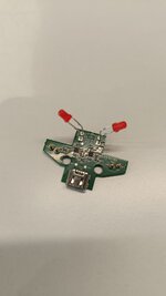
We are working on Charging Dock one of my hoby poject where we are using one of the Charging IC LGS4056

I used 2 Pogo pin to charge my device. But due to some issue this IC got damanged some time.

Do i need to add some protection ic in desgin at USB and Pogo pin side .

1710759686637.png
 
Hi,

how does your setup look like by means of actual layout and connection to the cell?
Which IC is actually used? The schematic shows the LGS4054 and in the text you mention the LGS4056.
How does the handling look like when a damage occures, is it "reproduceable"?

According to the datasheet of the LGS4056 it seems it can widthsand ESD pulses according to the HBM and CDM, at least I would intreprete it like that. Unfortunately I could only find a chinese (?) datasheet. The VCC as well as the CE pin can handle voltages up to 28 V, so they should not be prone to EMC events "that-much". Or at least they can handle a "higher" voltage. Nevertheless, if using an USB wall-plug supply, disconnecting the supply may course high transients. You may place a TVS diode in the vicinity of the USB connector to limit this voltages e.g. SMAJ5.0A/AC.

The 10 µF capacitor at the input of VCC should be for sure large enough to eat up the charge introduced by ESD. Here, the effectiveness depends on the location of the capacitor. For ESD purposes it should be placed close to the USB connector especially befor splitting up into individual traces e.g. towards CE. Here the 10 µF is used as a buffer, and should be plced close to the VCC pin. You might place an additional 100 nF with a 100 V rating close to the USB connector.

The BAT pin has a maximum voltage rating of only 6 V, so also here the 10 µF capacitor should be more than sufficient to limit the voltage by an ESD event. What's the voltage rating of this capacitor? Also here, the capacitor should be placed close to the connector.

What you should keep in mind is the power dissipation of the IC, as you have set your charging current to 0.5 A. Starting at a VBAT volatage of ~2.75 V, a current of 500 mA is delivered (Figure 9 in the DS). With a supply voltage of 5 V, this would lead to a power loss of about (5 V - 2.75 V) • 0.5 A = 1.125 W. I could not find any information regarding the thermal resistance in the datasheet, but here you can find the junction-to-ambient information for a DFN 2x2 and 3x3. Depending on your used package, the temperature rise is quite high. I could not figure out if the LGS4056 also has a thermal regulation to protect itself. Also keep in mind, the thermal resistance stated in the link, as well as in every other datasheet is highly depending on the actual layout (effective copper area; VIAs; ....) and number of layers and of course if natural or forced convection is applied.

So please show us your design/layout and share the english datasheet if you have it for the CORRECT part number.

BR
Hi,

Thank you for reply.

I understood the USB connector side; i must add the TVS diode or else a 10 uF capacitor.

I am attaching the English version of the LGS4056. I think it will be helpful.
 
Attachment or Link is missing.

Please also show a photo of your setup.
Please show us your Layout.

BR
 
Here is the Image of PCB and also the EN version of the datasheet
 

Attachments

  • WhatsApp Image 2024-03-27 at 11.47.58 AM.jpeg
    WhatsApp Image 2024-03-27 at 11.47.58 AM.jpeg
    50.9 KB · Views: 35
The battery wires will add about 10 nH/cm and the pogo pins may bounce quickly into the low ESR battery and may create excessive high voltage with a fast rise time., so I suggested two low pF diodes to clamp to the charger rails or TVS. OK?

I don't know what ESD exposure you had, but this could be worse with more overvoltage energy.

I'm not sure. Any other opinions?

Again your link failed to appear but I showed it before.

BAT, CHRG ................................................– 0.3V to 10V

9V TVS https://www.vishay.com/en/product/85881/
 
Last edited:
Hi,

Have you checked/protected for inductive flyback on Pogo Pins?

I still do not get how the described circuitry/setup might be damaged by an inductive flyback. The simulation below shows the actual volatges at different points along the inductive connection towards the cell, as I understood the charging circuitry. Here, the back-to-back MOSFETs are used on purpose to show a more realistic opening, which is actually represented by the disconnection of the pogo-pins. Here, the red curves show the result for the 10 µF capacitance. Of course, the shown simulation result is based on assumptions, and the inductances as well as the charging current has been chosen too large for demonstration purposes.

BATTERY_CHARGER_PROTECTION.png


This is for sure the wrong datasheet. Have a look on the schematic in post #1 and compare the pins names. I linked a chinese datasheet in reply #2.

For the example in reply #7 with the LTC4056, I see a possible hazard, and the proposed circuitry should protect the LTC4056.

I don't know what ESD exposure you had, but this could be worse with more overvoltage energy.
Here we have to differentiate ESD and EMC, where an ESD event usually represnts a high voltage (in the kV range) but with less energy. For testing, usually a capacitor in the low 100 pF range is charge up (kV) and discharged via a resistor in the 1 kOm range. By providing a large valued capacitor at the entrance of the PCB (connector), with a propper voltage rating, this will simply result in a low voltage at the DUT. Basically the charge at the DUT has to be the same as the one introduced by the ESD tester (gun) --> Q_ESD = Q_DUT --> V_DUT • C_DUT = V_ESD • C_ESD --> V_DUT = V_ESD • C_ESD / C_DUT.

I agree, any high energy source will worsen the situation.

BR
 
This thread raised more questions for me.
  1. What happened to your links? Script blocker?
  2. Which P/N is correct? given that I don't see an LGS4054H
  3. Which OEM datasheet has the same part which failed?
  4. Which port failed and how short or open? or no current?
  5. Are there any ESD specs for your part? I don't see any.
  6. Was there a thermal issue given you did not use an NTC protection recommended by www.legend-si.com LGS4056 doc.

Upon reflection I change my recommendation to small Caps on both ports.
Since ESD energy is modeled by only 100 or 200 pF any low ESR cap ceramic or e-cap will shunt ESD or flyback voltage by I*ESR and slew rate is not an issue for voltage, only dI/dt current and Vmax. For some reason , They chose two 10uF caps perhaps std ESR (>10 ohms) and not low ESR >0.1 ohm for 10uF.
.
I suggest thermistor be included if there is no CC shutdown due to excessive battery leakage (>C/10) or shorted cell.

Other causes possible but unknown.
1711588308042.png
 
Last edited:
Hi,

please share the ENGLISH datasheet. It's not possible to copy the text out of the chinise one I linked in reply #2, so no change to translate it.

I suggest thermistor be included if there is no CC shutdown due to excessive battery leakage (>C/10) or shorted cell.
To me it looks like the intention of the NTC is to protect the cell i.e. against thermal run-away. So it should be placed in the vicinity of the cell itself, but the battery holder is not located on the PCB. So a wired solution has to be used. For sure the NTC can be used in a way to protect the IC itself, or a smart combination of to do both, cell and IC. But as I'm not able to read the DS, I can not give any further advise on that.

My concerns about the IC's power dissipation I pointed out already in reply #2, and there already for the designed charging current of 500 mA. In reply #2 I already asked to share the LAYOUT. On the provided picture it is hard to judge on the thermal "performance" of your design e.g. the bottom side would be of interest too.

BR
 
translation "
TEMP: When the battery temperature sensing function is not needed, it is recommended to short-circuit this pin to GND to avoid interference. (TEMP is suspended and grounded, and the NTC function is canceled) Select different resistance values according to the battery detection temperature threshold. For other NTC resistance models, please contact Prism AE for consultation.
--- Updated ---

It occurred to me that this IC may have failed from oscillation thermal failures in the battery charge operation. As some sort of linear amplifier it is prone to oscillations from voltage and current feedback under some large capacitive loads (>> 1kF) presented by batteries.

So it is curious if this may explain your unexpected failures. There are generally a couple methods to avoid instabilities; use phase lead compensation for negative feedback (not possible) or snub the RF response to prevent oscillations with extremely low ESR. Normally I say caps in this range are low ESR if Tau is from 1 to 10 us meaning ESR*C=Tau. Some excellent caps are lower, as in the case for this OEM chip maker has a demo board which shows two Samsung 10 uF caps on both input and output ports in parallel (1210 case)

The Samsung caps used have ESR= 0.05 ohms or Tau=0.5 us = ESR*C. Using two caps in parallel on both ports suggests it must be for IC performance, and not simply ripple reduction.
1711643383264.png

--- Updated ---

This also reminds me that if using thermal sensing, it is also a bad for the battery life to put hot used cells in a charger right away as the high ESR promotes more self heating on a depleted cell which acclerates aging.
 
Last edited:

LaTeX Commands Quick-Menu:

Part and Inventory Search

Welcome to EDABoard.com

Sponsor

Back
Top