Continue to Site

Welcome to EDAboard.com

Welcome to our site! EDAboard.com is an international Electronics Discussion Forum focused on EDA software, circuits, schematics, books, theory, papers, asic, pld, 8051, DSP, Network, RF, Analog Design, PCB, Service Manuals... and a whole lot more! To participate you need to register. Registration is free. Click here to register now.

Timing question with combinational gates

Qwerty112233

Member level 2
Joined
May 21, 2021
Messages
43
Helped
1
Reputation
2
Reaction score
2
Trophy points
8
Activity points
368
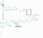
When we have let's say, NAND gate on clock path..does that change timing edges and checks for setup and hold?

Seeing a rise edge flop that is getting timed at falling edge for hold..but it shows NAND cell in the path so i'm curious how these non buffer/inverter clock logic cells change timing?
 
In general, this is not the behavior that the tools implement in the clock tree. They typically keep the same clock polarity. It might be possible that what you are describing is enabled by some advanced setting, but I cannot be sure.
 
Ah, I looked at the path closer and found that clock path started with falling edge because there's a XNOR gate inverting polarity in the clock arc. Trying to understand what needs to be done wrt clock path cells.
 

Attachments

  • SmartSelect_20231004_142740_Samsung Notes.jpg
    SmartSelect_20231004_142740_Samsung Notes.jpg
    187 KB · Views: 54
Hi,

This is what you should avoid.

You should feed the global clock to the DFF and do the rest with the DFF_enable.
This is why there is a global clock.

Klaus
 

LaTeX Commands Quick-Menu:

Part and Inventory Search

Welcome to EDABoard.com

Sponsor

Back
Top