Continue to Site

Welcome to EDAboard.com

Welcome to our site! EDAboard.com is an international Electronics Discussion Forum focused on EDA software, circuits, schematics, books, theory, papers, asic, pld, 8051, DSP, Network, RF, Analog Design, PCB, Service Manuals... and a whole lot more! To participate you need to register. Registration is free. Click here to register now.

[SOLVED] OPA847 oscillating in high frequency.

Status
Not open for further replies.

Karolina_1

Member level 3
Joined
Mar 10, 2017
Messages
67
Helped
0
Reputation
0
Reaction score
1
Trophy points
8
Activity points
639
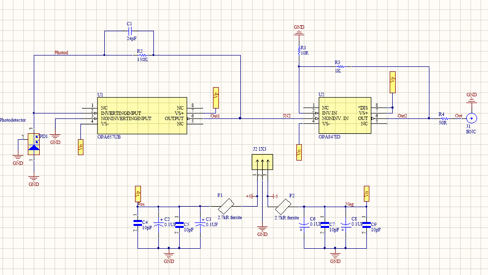
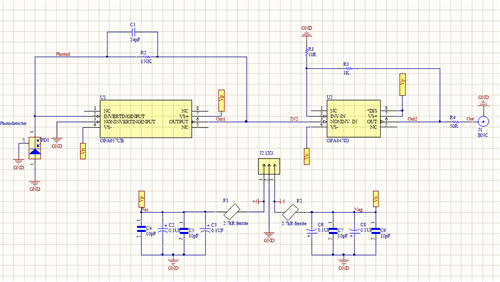
Hello Everyone? I have an oscillation issue on a photodiode trans-impedance amplifier whose simplified schematic I'm attaching in this thread. The design consists of a high gain / high bandwidth trans-impedance stage using a JFET Input OPA657 (SOT23-5 Package), followed with a voltage gain of 101V/V made with an OPA847 (SOT23-6 Package). All components used are SMD technology. Transimpedance stage works fine, OPA657 is functioning good, however, there is a high-frequency oscillation at the output of the OPA847. For that reason, I am only testing the OPA847 part(OPA657 is removed). I connected the signal generator to the non-inverting input of the OPA847. In tests, I am inputting 100mVpp, 50Hz signal. And I am using 40R and 1000R resistances (gain 21V/V) and measuring the voltage after 50R resistance.

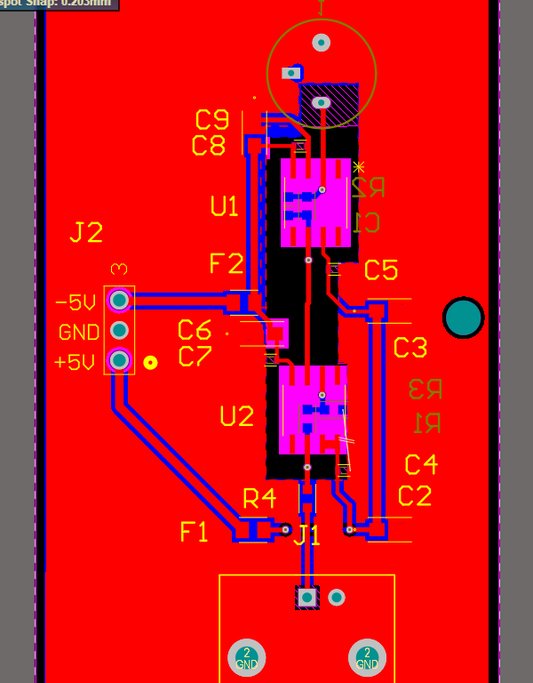
Opamp has 2 bypass capacitors on each supply pin (0402/10pF - Ceramic, 1206/100nF Tantalum) and ferrite bead on each supply pin of the opamps (Murata BLM21BD272SH1L). All of them are very close to the pins. I followed all the indications on the application notes of each opamp to make the entire PCB. The implementation was made in a 2 layer, FR4 PCB.

The circuit oscillates around 20 MHz. Here are the things I tested to figure out what kind of problem I have (without success):

1. Putting the 10uF Aluminium electrolytic capacitor.
2. Removing 0402/10pF - Ceramic cap and replacing them with 0603/0.1uF Ceramic cap.
3.Using different power supply.
4. Putting 10R resistance in series with both negative and positive power pins.
5. Changing different resistor combinations, so that gain>20V/V.
6. Replacing OPA847.
It's not an ambient pick-up when power off the high freq oscillation goes away.


Are you looking at output pin or 50 ohm BNC jack ?

Scope probe, X 10 right, not X1. Big difference in C load from probe. Probe
ground lead going where ?

**broken link removed**


What node is most sensitive to taking a 1 K R, one end in your fingers, the other
a probe point, and walking it around the circuit while watching scope ?


Regards, Dana.
 

OP847 datasheet states "STABLE FOR GAINS ≥ 12". It's not suited for transimpedance amplifier, or at least not with the given circuit dimensioning.
 

Are you looking at output pin or 50 ohm BNC jack ?

Scope probe, X 10 right, not X1. Big difference in C load from probe. Probe
ground lead going where ?

**broken link removed**


What node is most sensitive to taking a 1 K R, one end in your fingers, the other
a probe point, and walking it around the circuit while watching scope ?


Regards, Dana.

Hi, Dana. I am measuring after the 50R and before the BNC jack(I removed BNC, there is just a test point). When I use 1X there is 20MHz oscillation and when 10X used, its 26MHz. And when I use BNC to crocodile connector there is 12MHz oscillation.

I was not able to understand,
What node is most sensitive to taking a 1 K R, one end in your fingers, the other
a probe point, and walking it around the circuit while watching scope ?


you mean I should hold one side of 1kR resistor and connect the other size to the probe's ground and test circuit at different places.

I am using signal generators to input 100Hz, 100mVpp signal into the non-inverting input of the OPA847.

Kind regards,
--- Updated ---

OP847 datasheet states "STABLE FOR GAINS ≥ 12". It's not suited for transimpedance amplifier, or at least not with the given circuit dimensioning.

My gain is higher than gain>21V/V. Why it is not suitable for given circuit dimensioning? It is used as an amplifier. OPA657 is used as a trans impedance.
 
Last edited:

Sorry for the confusion, I thought OPA847 was used for the first stage. In the second stage, I see this possible problems:
- trace between OP and bypass capacitor too long
- missing stitching vias betwen top and bottom copper pour. Bypass capacitors and R1 have no direct connection.
 

Where are thru Vias ?? The layout is bad.
 

Look at datasheet for ceramics you are using. Not all manufacturer .01 and .1
uf caps have the same esr performance. Also .1 uf crap out at realatively low
freq, consider a .01 and .1 in parallel.

I cannot emphasize enough look at datasheets, i have seen some cermaics
that were markedly worse in bypoass performance.

A good way of telling is set up a jig on bafe PCB and use a VNA to look at it.


Regards, Dana.
--- Updated ---

Fix probe to output, ground lead to ground.

Hold one end 1K R in finger, use the other as a probe. What you are doing is loading nodes you
touch with C. One node that has significant effects will be the Inv input of OpAmp. Because
C and the fdbk R add phase lag to the loop, a recipe for instability. That should also lower osc
freq.

Note this includes touching power leads of OpA,mp right at package.


Regards, Dana.
 
Last edited:

Sorry for the confusion, I thought OPA847 was used for the first stage. In the second stage, I see this possible problems:
- trace between OP and bypass capacitor too long
- missing stitching vias betwen top and bottom copper pour. Bypass capacitors and R1 have no direct connection.
Hi, as in the picture, I tried to put bypass capacitors as close as possible to the power pins of the opamp(I replaced 1206 tantalum capacitors with 10uF alum electrolytic cap). There are electrical connections between the top and bottom polygon pour (shown with yellow, they are connected in multiple places, in the PCB layout that I shared, the via in the positive cap polygon is not seen, but it is there shown with red). R1 (feedback) and R3 resistors are on the bottom layer, does being in the bottom layer considered as indirect connection, does it mean that R1 and R3 must on the top layer.

IMG_20200708_090350.jpg

--- Updated ---

Where are thru Vias ?? The layout is bad.
Hi, BigBoss, I replied to your message above. There are 7 connections between the top and bottom polygon pour. There was a problem with the layout I shared. On the positive bypass capacitor connected to the ground, there seems to be a via missing, and the cap is not connected to the ground. But it is there, as in the picture I shared above.
 
Last edited:

Hi,

Electrolytics capacitors are worse than tantals and are generally not suitable as bypass capacitors for high frequencies (like here to prevent from some megahertz oscillations).
Your capacitor need to be suitable for those megahertz frequencies.
Thus the "usual bypass capacitor" is a 100nF ceramics.

The electrolytics should be used as bulk capacitor in parallel to the bypass capacitor.

"Electrical connections" tells me that you rather think DC, but you need to think in HF. Megahertz is your target (to prevent oscillations).
Lengthy wiring, every trace, every return path will cause inductivity...and this inductivity combined with megahertz frequency cause a lot of impedance.
Maybe the umpedance is high enough to make the "connection" useless to prevent oscillations.

--> a solid GND plane with independent vias is what you need.
A copper pour is no GND plane! It's not much benefit against simple traces...because HF does not care much about (trace) width.
It cares about the loop size, enclosed loop area (and others)...

There are many discussions about this ...just do a forum search

Klaus
 

Look at datasheet for ceramics you are using. Not all manufacturer .01 and .1
uf caps have the same esr performance. Also .1 uf crap out at realatively low
freq, consider a .01 and .1 in parallel.

I cannot emphasize enough look at datasheets, i have seen some cermaics
that were markedly worse in bypoass performance.

A good way of telling is set up a jig on bafe PCB and use a VNA to look at it.


Regards, Dana.
--- Updated ---

Fix probe to output, ground lead to ground.

Hold one end 1K R in finger, use the other as a probe. What you are doing is loading nodes you
touch with C. One node that has significant effects will be the Inv input of OpAmp. Because
C and the fdbk R add phase lag to the loop, a recipe for instability. That should also lower osc
freq.

Note this includes touching power leads of OpA,mp right at package.


Regards, Dana.

Hi Dana, I will use .01 and .1 in parallel next time, keeping in mind the ERS values from Datasheet and making sure they are suitable to be used as bypass capacitors.

As you said I loaded nodes with C using 1kR and hand. The 20MHz decreased to 19.8MHz. What should I conclude from this?
--- Updated ---

Hi,

Electrolytics capacitors are worse than tantals and are generally not suitable as bypass capacitors for high frequencies (like here to prevent from some megahertz oscillations).
Your capacitor need to be suitable for those megahertz frequencies.
Thus the "usual bypass capacitor" is a 100nF ceramics.

The electrolytics should be used as bulk capacitor in parallel to the bypass capacitor.

"Electrical connections" tells me that you rather think DC, but you need to think in HF. Megahertz is your target (to prevent oscillations).
Lengthy wiring, every trace, every return path will cause inductivity...and this inductivity combined with megahertz frequency cause a lot of impedance.
Maybe the umpedance is high enough to make the "connection" useless to prevent oscillations.

--> a solid GND plane with independent vias is what you need.
A copper pour is no GND plane! It's not much benefit against simple traces...because HF does not care much about (trace) width.
It cares about the loop size, enclosed loop area (and others)...

There are many discussions about this ...just do a forum search

Klaus

Hi, Klaus, here as you said I am using 0.1uF ceramic and 10uF Electrolytic capacitor in parallel as a bypass, does the size of 0.1uF matter (0603, 0805, 1206). Solid ground plane you mean ground polygon pour with multiple vias. (There are actually 7 points connecting top and bottom grounded copper polygon pours in my design). This copper pour is connected to the ground.
 
Last edited:

your freq source went down by .2 MHz, 10nF & 100nF & 1uF quality MLCC caps right on the supply pins are always needed for proper performance - decouple each op-amp supply too for best behaviour ...
 

The minimal drop C brings on nodes indicates the stray C
on nodes already dominant in problem, that no node seems
to be sensitive to C loading change. You can try exercise again
with 100 ohm R. As R goes up your reflected body C goes down
that is applied to nodes.

On caps its the ceramics that will make the difference at 20 Mhz.
Tants, polymer tants (the best versions) have higher ESR at
20 Mhz, losing ground.

1594200823714.png


Regards, Dana.
 

    Karolina_1

    Points: 2
    Helpful Answer Positive Rating
your freq source went down by .2 MHz, 10nF & 100nF & 1uF quality MLCC caps right on the supply pins are always needed for proper performance - decouple each op-amp supply too for best behaviour ...

There is 0.1uF 0603 ceramic, 0.1uF tantalum, and 10uF alum electrolytic cap. on positive and negative supplies. Additionally, there is also a ferrite bead. BLM21BD272SH1.
--- Updated ---

The minimal drop C brings on nodes indicates the stray C
on nodes already dominant in problem, that no node seems
to be sensitive to C loading change. You can try exercise again
with 100 ohm R. As R goes up your reflected body C goes down
that is applied to nodes.

On caps its the ceramics that will make the difference at 20 Mhz.
Tants, polymer tants (the best versions) have higher ESR at
20 Mhz, losing ground.

View attachment 162758


Regards, Dana.
Thanks, Dana, I exercised with 100R and directly with hands. There is a very small freq change, almost not noticeable. The frequency is changing constantly between 20.4-20.9MHz.

I removed 10uF elec and 0.1uF tant cap and put 10uF ceramic cap. The oscillation continues, unfortunately.
--- Updated ---

This is the second prototype of the photodetector board. Are there any mistakes in the PCB layout? If I won't be able to solve the OPA847 oscillation problem, I will have to replace it with ADA4895 or AD8675 or THS3091.
Capture1.PNG
Capture3.PNG
Capture2.PNG
 
Last edited:

I don't like the lack of gnd panes under the IC's and the caps for Vcc are too far away ...


Hi,

Solid ground plane you mean ground polygon pour with multiple vias. (There are actually 7 points connecting top and bottom grounded copper polygon pours in my design). This copper pour is connected to the ground.
One layer of solid GND is sufficient. Solid means: Without other traces, without cuts.
I call "copper pour" as almost useless regarding HF. It can neither replace a GND plane nor truely support a GND plane...in most cases.
Why: I've already explained in many other threads. Just do a forum search.

Klaus


how do you know it is well functioning? - have you bought one and tried it ...?
 

how do you know it is well functioning? - have you bought one and tried it ...?

No, but they wouldn't sell unless it's operational? I am trying to solve my problem. Your advice and help are highly appreciated and but I don't want to have an argument with you.
 

Status
Not open for further replies.

Similar threads

Part and Inventory Search

Welcome to EDABoard.com

Sponsor

Back
Top