Continue to Site

Welcome to EDAboard.com

Welcome to our site! EDAboard.com is an international Electronics Discussion Forum focused on EDA software, circuits, schematics, books, theory, papers, asic, pld, 8051, DSP, Network, RF, Analog Design, PCB, Service Manuals... and a whole lot more! To participate you need to register. Registration is free. Click here to register now.

[SOLVED] OPA847 oscillating in high frequency.

Status
Not open for further replies.
Have you posted over at Analog Devices forum, or contact their sales
office, just to make sure there is not a bad batch of parts out there. The
testing you did loading C onto various nodes with little change in freq
indicates to me its part internal issue. If there is a bad batch they should
be able to supply data codes of problem part runs.

Regards, Dana.
 

    Easy peasy

    Points: 2
    Helpful Answer Positive Rating
Thanks for the feedback Dana, I posted on the TI forum https://e2e.ti.com/support/amplifiers/f/14/p/916824/3398364#3398364 but was not able to solve my problem. Many people have this problem, the majority solved their high-frequency issue by:
1. Putting 50R at the output pins and measuring after the 50R.
2. Making gain higher than 21V/V.
3. Putting ferrite beads.
4. Trying different combinations of bypass capacitors.

As I said I removed the OPA657(transimpedence) and I am testing OPA847(amplifier part) as its seen in the picture I shared. The signal from the signal generator was connected to the non-inverting input of OPA847. And I was measuring after 50R at the output of the opamp.

I put 100R in series and 1nF ceramic cap (forming LPF) at the non-inverting input. The high-frequency oscillation is gone and it's amplifying correctly. However, LPF is limiting my BW which is not desirable.
 

I put 100R in series and 1nF ceramic cap (forming LPF) at the non-inverting input. The high-frequency oscillation is gone and it's amplifying correctly.
Suggests that the instability is caused by the combination of amplifiers, respectively insufficient bypassing of the combi.
 

    Karolina_1

    Points: 2
    Helpful Answer Positive Rating

    Easy peasy

    Points: 2
    Helpful Answer Positive Rating
Suggests that the instability is caused by the combination of amplifiers, respectively insufficient bypassing of the combi.
I actually removed the OPA657 and testing OPA847 only with signal generator inputting from non-inverting input of opamp and measuring after 50R with an oscilloscope. As you said I tried different combinations of capacitors as the bypass but it, unfortunately, didn't help. Maybe the problem is in the layout?
 

Can be a layout problem. I would try vias (may be implemented as drilled holes with wires soldered at both sides) next to each high frequency bypass capacitor + R1 and a jumper wire across the central ground pour gap.
 

    Karolina_1

    Points: 2
    Helpful Answer Positive Rating
New layout looks more promising.Pay attention to de-coupling capacitors ( they might be closer to IC ).
Add mode VIA closer to GND pins of de-coupling and make them as close as possible to ICs.
 

    Easy peasy

    Points: 2
    Helpful Answer Positive Rating

    Karolina_1

    Points: 2
    Helpful Answer Positive Rating
New layout looks more promising.Pay attention to de-coupling capacitors ( they might be closer to IC ).
Add mode VIA closer to GND pins of de-coupling and make them as close as possible to ICs.
Thank you, I will move de-coupling cap closer to the pins and add vias close to their ground connection and share the last version. I hope this time caps are close enough.
--- Updated ---

Can be a layout problem. I would try vias (may be implemented as drilled holes with wires soldered at both sides) next to each high-frequency bypass capacitor + R1 and a jumper wire across the central ground pour gap.
Thank you, I made them closer and put vias near caps and R1 ground connection. Put jumper wire across the central pour gap, I understood as connecting regular breadboard jumper wire to ground on both sides and laying it over the central gap.
--- Updated ---

I put caps closer to the input power pins of the OPAMP and vias near the cap ground connection.
Capture.PNG
 
Last edited:

Nice ..
When you design a PCB, pay attention generally few things mentioned below..
-Grounding
-Symmetry
-Decoupling

Fill the proper spaces with VIAs, no problem occurs..
Also, shielding will help you to protect the circuit against EMI.
 

    Karolina_1

    Points: 2
    Helpful Answer Positive Rating
I noticed that before I connect the probe to the output, and measure the ground, there is an oscillation at (1kHz from the signal generator to non-inv input of opamp) at around 1kHz(very noisy). when I connect the probe to the output of the opamp and probe the ground there is 20MHz oscillation. Is it useful information 🙃
 

Can you do scope screen captures and pics of actual board and probing
for the pics ? Model of scope and probe ?


Regards, Dana.
 

Hi,

And we need to see the scope setup.

Klaus
 

Can you do scope screen captures and pics of actual board and probing
for the pics ? Model of scope and probe ?


Regards, Dana.
f345fd95-e570-4d53-a2ab-32fbe445d3c6.jpg
dceaa9cf-603b-469b-8b96-97c30187038c.jpg
2b473f80-1ed3-4cde-b40d-d2263734f621.jpg


--- Updated ---

Hi,

And we need to see the scope setup.

Klaus

Coupling-AC (tried also DC but doesn't change)
BW limit-OFF
Invert-OFF
Probe-1.00:1
Skew-0.0s
Units-Volts
--- Updated ---

Have you tried remove ferritebead on negative side ?
Yes, I tried removing negative, positive, and both.
 

Attachments

  • ffa0b909-eb78-4339-8b05-c1a9872aee01.jpg
    ffa0b909-eb78-4339-8b05-c1a9872aee01.jpg
    102.4 KB · Views: 149
Last edited:

Hi,

I neither can't see the numbers on your scope, nor is the timing setup useful to recognize the waveform.

Klaus
 

Hi,

It looks like you are possibly using 'the pointy hat'/'the witches hat' for the ground probe connection. Not recommended.

Power Tip #6 (see figure 2)

Short Ground Leads (see figure 7)
 

    Karolina_1

    Points: 2
    Helpful Answer Positive Rating
why is there a big hole in the gnd plane under the chips ... ?
--- Updated ---

and 10uf MLCC on the board for the supply ... ?
 

Hi,

It looks like you are possibly using 'the pointy hat'/'the witches hat' for the ground probe connection. Not recommended.

Power Tip #6 (see figure 2)

Short Ground Leads (see figure 7)
You are a lifesaver d123 :D 
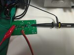
. I connected the probe as shown in the figure and I was able to see it. However, there was a noise. I tried using a similar probe to connect the non-inverting input of the OPAMP and the noise is very low. So the whole problem was about connecting the probe properly. Big thanks to everyone who has been helping me. Your help was very much appreciated.
--- Updated ---

why is there a big hole in the gnd plane under the chips ... ?
--- Updated ---

and 10uf MLCC on the board for the supply ... ?

These holes were meant to used to mount the card to the board or box.

My 0.1uF and 10uF caps are X7R 10% 25V 0603 and X7R 5% 16V 1206 respectively.
 
Last edited:
perhaps you are dyslexic? hole in the gnd plane under the chips ...
Maybe if you use correct terms people will understand you. what do you mean by hole, there are many types of holes(via is also a hole), be more specific. Do you mean "polygon cut out"? So far you have been useless, maybe you should just not write here.
 

Status
Not open for further replies.

Part and Inventory Search

Welcome to EDABoard.com

Sponsor

Back
Top