yuxiaojian01
Newbie level 4
Hi everyone,
I am using IBM 130nm cmrf8sf PDK. I made a simple inverter and performed DRC, LVS, PEX with Calibre. The DRC and LVS work well, but there is a PEX error shown as follows:
"error: Could not find pin mapping for terminal sub of cell (cmrf8sf devicepad symbol). It will remain unconnected."
I don't quite understand this error, could anyone can explain this error and tell me how to solve this problem?
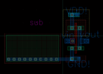
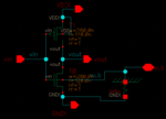
In the circuit, I added a "sub" terminal in the schematics and a "sub" label (with SXCUT ll layer), which represents the substrate.
I also attached the schematics and layout. In the layout, the left instance is a subc instance copied from cmrf8sf library.


