imrankhanPNU
Member level 1
Hello,
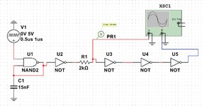
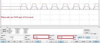
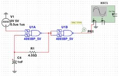
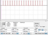
I'm modulating the message signal with OOK (on-off keying) modulation. Multisim software is used to model the schematic [attached]. At the resistor R1, the modulated signal is obtained. I wanted to invert the modulated single, for that I used a simple NOT gate (U3), however at the NOT's gate output, I got the same signal as input means without inverting [attached]. So my question is, why isn't the NOT gate inverting? Am I doing something wrong?
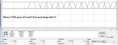
As hit and trail, I added two more NOT gates (U4 and U5) but this time I got an inverted signal, although further improvement is needed to achieve a 180-degree phase shift. So my second question is: Why is it an inverter this time? and how to get exactly a 180-degree phase shift between two signals?
Thanks for your time.
