Janecheck
Newbie level 5
Hello,
I am getting distored signal on HO output of my IR2110 driver.
I connected my IR2110 driver to a pair of two n - channel IRFP250 MOSFETs (no load) same as shown in data sheet.
I did not add the capacitor between drain of high side MOSFET, and source of low side MOSFET.

Picture 1 The way I wired the circuit (but without capacitor on the right side of the MOSFETs)
I used:

Picture 2 Setup
I supplied it with a 12V DC and used Arduino Uno as square wave signal source.
Arduino code
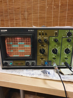
Then I measured LIN, LO and HIN, HO with oscilloscope. Here are the measurments:
LO (top) & LIN (bottom)

Picture 3 Signals from LO (top) and LIN (bottom)
It looks good.
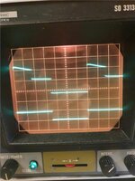
HO (top) & HIN (bottom)

Picture 4 Signals from HO (top) & HIN (bottom)
As we can see the signal from HO is distored and I don't know why. What might be the issue?
Is it because I picked wrong capacitor between Vb and Vs? If yes then how to choose the right capacitor?
I am trying to make 3 - phase inverter. At first for testing purposes only I wanted to control the speed of BLDC motor but after wiring it up it had quite a big problem to spin (it stared spinning after I pushed it a bit) and also one of six MOSFETs got hor quite fast (he is okay he just heats pretty quickly and this was strange for me). Now after measuring with oscilloscope I believe that the distorted HO signal was the issue.
Please help me.
I am getting distored signal on HO output of my IR2110 driver.
I connected my IR2110 driver to a pair of two n - channel IRFP250 MOSFETs (no load) same as shown in data sheet.
I did not add the capacitor between drain of high side MOSFET, and source of low side MOSFET.
Picture 1 The way I wired the circuit (but without capacitor on the right side of the MOSFETs)
I used:
- 3 x 100 nF ceramic capacitors
- 2 x 100 ohm resistor
- 1 x UF4007 diode
Picture 2 Setup
I supplied it with a 12V DC and used Arduino Uno as square wave signal source.
Arduino code
Code:
digitalWrite(3, HIGH);
digitalWrite(5, LOW);
delay(5);
digitalWrite(3, LOW);
digitalWrite(5, HIGH);
delay(5);
Then I measured LIN, LO and HIN, HO with oscilloscope. Here are the measurments:
LO (top) & LIN (bottom)
Picture 3 Signals from LO (top) and LIN (bottom)
It looks good.
HO (top) & HIN (bottom)
Picture 4 Signals from HO (top) & HIN (bottom)
As we can see the signal from HO is distored and I don't know why. What might be the issue?
Is it because I picked wrong capacitor between Vb and Vs? If yes then how to choose the right capacitor?
I am trying to make 3 - phase inverter. At first for testing purposes only I wanted to control the speed of BLDC motor but after wiring it up it had quite a big problem to spin (it stared spinning after I pushed it a bit) and also one of six MOSFETs got hor quite fast (he is okay he just heats pretty quickly and this was strange for me). Now after measuring with oscilloscope I believe that the distorted HO signal was the issue.
Please help me.