Continue to Site

Welcome to EDAboard.com

Welcome to our site! EDAboard.com is an international Electronics Discussion Forum focused on EDA software, circuits, schematics, books, theory, papers, asic, pld, 8051, DSP, Network, RF, Analog Design, PCB, Service Manuals... and a whole lot more! To participate you need to register. Registration is free. Click here to register now.

If anybody need help in EAGLE, ask me in this POST !

Status
Not open for further replies.
The L298 is in the st-microelectronics library. The easy way to find devices is to "select all" for you libraries then use the wildcard search when placing a component.

Keith.
 

reymund said:
is there a library for a multiwat package, like for the l298 motor driver??, where can i find it, and how to make the pads of the elements, to have holes n its center, for the drilling, mines dont have thanks.....
What do you mean with "yours doesn't have holes"? Do you mean the pads or the big center hole for mounting the chip horizontally?
If you mean the holes in the pads, can't you see them in the library or in the board?
Btw. the Eagle library only contains the vertical version.
 

Hi
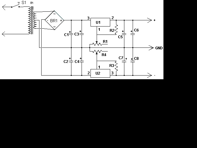
I wonder how to connect the potentiometer in eagle , and how to connect it ? , the circuit I'm working on , in this link ,
supply3.gif


also I'm going to do this project using 8085 microprocessor , so does eagle have this chip in its library ?
thanks ,
 

i already saw it, my config is, my pads on the components dont have drill holes, now, is there any package on l298?, it is a multiwatt package. thanks
 

As I said in my post yesterday "The L298 is in the st-microelectronics library."

Keith.
 

Is there a way to create a custom device that contains a symbol, but no package?

I'm trying to do this intentionally so I can I have a circuit that is shown on the schematic as a reference but will not be converted into a board layout when it comes to PCB layouting.

If that isn't possible, a way to make sections of the schematic "unboard-able" is also a valid solution.

Any ideas?
 

Yes, it is perfectly possible. The "frames" and supply symbols are two examples which don't appear on the board. Simply create them in the normal way (make a symbol & create a device) but when you create the device you simply don't add a package. Open up the supply or frames libraries to see how it is done.

Keith.
 

IC that i want to designe

HI
thanks for ur helps but please tell me ,how can i design an IC package if it's not in the libraries?...i attache the IC ...I'll be very grateful if you helped me in designing it
 

There is a tutorial here:


You should be able to copy the PCB footprint from one of the libraries - there are most standard footprints in the smd-ipc library and possibly some other libraries. So then you would just need to create the symbol & connect the two together in a "part". Otherwise you will also need to create the footprint.

You can also copy the footprint from any other library if another Analogue Devices part uses it. Be careful - Analogue Devices uses more than one pitch of CSP package. What is the part number of the device? You can find a lot of extra devices here, uploaded by other users:


Keith.
 

I had a net in the schematic which maps to a wire on the PCB. Then I realized the wire (complicated antenna shape) required two nets. Unfortunately, that means I have to ripup half the antenna, and redraw it to assign it to a new net. Is there not a way to just split the wire, and assign half of it to a new net without redrawing?

Thanks!
 

It is tricky to be specific without the files and a diagram, but it should be possible. Backup your .sch and .brd files first. I think you need to separate the PCB and schematic to do it. So close the schematic and split the PCB track. Then you have to load the schematic and try to get it synchronized again. One half of the antenna will have acquired a new net name. You now need to split the schematic net and give the two halves names which match the PCB tracks or vice versa.

If it all goes horribly wrong and you cannot sort it out, use you backups and try again.

Keith
 

keith1200rs said:
It is tricky to be specific without the files and a diagram, but it should be possible. Backup your .sch and .brd files first. I think you need to separate the PCB and schematic to do it. So close the schematic and split the PCB track. Then you have to load the schematic and try to get it synchronized again. One half of the antenna will have acquired a new net name. You now need to split the schematic net and give the two halves names which match the PCB tracks or vice versa.

If it all goes horribly wrong and you cannot sort it out, use you backups and try again.

Keith

Thank you! That worked. (For the record, CadSoft should provide an easier mechanism for this.)

Cheers! Zack
 

Zack,

I'm glad it worked. I don't know if there is a better way, but in my experience all PCB CAD packages have issues when it comes to maintaining the connection integrity between the PCB & schematic. Eagle tends to be very highly linked between the two. A lot of packages are more loose but you get involved in the netlist more. With either method you need to understand how it works. None of the packages are 'perfect'!

Keith
 

thanks alot

Keith you are fantastic ...I'm reading the Tutorial it looks wonderful..thanks alot

by the way the IC no. is ADL5322
 

I doubt you will find that part, but the package is probably in analog-devices.lbr. Be careful though - there is LFCSP8, LFCSP8_CP and LFCSP_VD08 in the library. One of them could be the correct one, but check it carefully.

Keith.
 

unfortunately there is nothing like 8-Lead Lead Frame Chip Scale Package [LFCSP_VD] in the library of the software...if you have it , please send it..I'll try to make the symbol..anyway thanks for your great helps.
 

What version are you using? This is from the version 5.8 libraries and has the packages I mentioned in it.

Keith.
 

what about the lines?

if i use components that work in the 800MHZ range should i do it with microstrip lines or it can be with normal lines ?
 

It depends! Have you 50 ohms impedances in the circuit? Is it RF or analog?

I do quite a bit of analog design up to 1GHz. In general, if you keep things short striplines aren't needed. In fact there often isn't much track to increase the width from the IC before you need to narrow it for the next one.

Sometimes a track of significant length is unavoidable so I would use a 50 ohm line.

Keith

Added after 1 minutes:

If you post your circuit (or PM me) I could comment specifically.

Keith
 

Hello Keith,

I am getting 113 of this warning:
"Close but unconnected wires in nets .."

What's the problem here ?!

Is it because I used wires then added junctions instead of using nets directly ?
 

Status
Not open for further replies.

Part and Inventory Search

Welcome to EDABoard.com

Sponsor

Back
Top