Continue to Site

Welcome to EDAboard.com

Welcome to our site! EDAboard.com is an international Electronics Discussion Forum focused on EDA software, circuits, schematics, books, theory, papers, asic, pld, 8051, DSP, Network, RF, Analog Design, PCB, Service Manuals... and a whole lot more! To participate you need to register. Registration is free. Click here to register now.

If anybody need help in EAGLE, ask me in this POST !

Status
Not open for further replies.
eagle to g-code

i'm trying to add a db9 male connector, but i cant find which library to use. thanks
 

hpgl.125 to gerber converter

rashad said:
i'm trying to add a db9 male connector, but i cant find which library to use. thanks

subd.lbr

sorry, is con-subd.lbr
 

autoplace with eagle

HELP!

I have a lot of SmartWork PCB file (ver 1.4r1, Wintek, USA).
I know this is an old program...

How do I import to EAGle these files?

SmartWork PCB > DXF or PCB > BMP, and dxf2scr or bmp2scr are working :)|) but I will "real import" !!

Thanks and best regards
zuisti (from Hungary)
 

pic24hj128gp502 eagle

Hello everyone!

How can we print the *.brd file without the devices being printed? I only want the pads and other components needed for pcb lay-out and for etching?

I tried printing it but the components were also included.

Help me!
 

eagle smd pad size

cloud said:
Hello everyone!

How can we print the *.brd file without the devices being printed? I only want the pads and other components needed for pcb lay-out and for etching?

I tried printing it but the components were also included.

Help me!
1. Click on the display button on the left side toolbar.
2. On the new window that appears, click "None" button and then select layers that you want to include in your print. Generally layers 16 , 17, 18 and 20 are used for single sided PCB (bottom side) and 1, 17, 18 and 20 are used for top side of double sided PCB.
3. Click OK and print your layout.
 

changing eagle autoroute parameters

Hi

I want to route few elements on the board. I wish to connect supply nets and data nets with different width using autorute.

tnx
 

eagle cad multiple sheet tutorial

Thanks CMOS!:D

You're always there to lend a hand to us newbies!

Another thing, how do we change the pads of the components when a default size is already in place?:?:
 

eagle library conectores db 9 db 32

cloud said:
Another thing, how do we change the pads of the components when a default size is already in place?:?:
Change the pad size in the corresponding library.
Back again in the board choose the menu item "Library / Update" and point to the changed library - that's it.
But this will change all components using that library ....
 

+eagle light +gerber

M!k said:
cloud said:
Another thing, how do we change the pads of the components when a default size is already in place?:?:
Change the pad size in the corresponding library.
Back again in the board choose the menu item "Library / Update" and point to the changed library - that's it.
But this will change all components using that library ....
To change the pad in the entire library....use "change-pad-in-lbr.ulp" ULP.
 

cadsoft eagle autoplace

Thanks a lot Mik and CMOS!

Hoping for your unending support to us. God bless and again, thanks a million!
 

eagle bmp importieren wire

This has probably been asked before, but ....

I believe there is a way of getting Eagle (I downloaded the latest free version) to produce a single-sided board.

Please give me some advice on how to do it.
 

rj11 connector eagle cad

Hello,

I'm designing different boards on which i'm always using the same layout for a particular RF part.

I'm wondering how I could integrate part of a layout (2cm square to fix the idea) in an eagle library? I know how to do that for SOIC, etc. components but don't know how to handle this for a symbol (just like in Cadence, ADS, etc...).

Anybody knows?
 

rj11 eagle cad

Hello, It's me again.

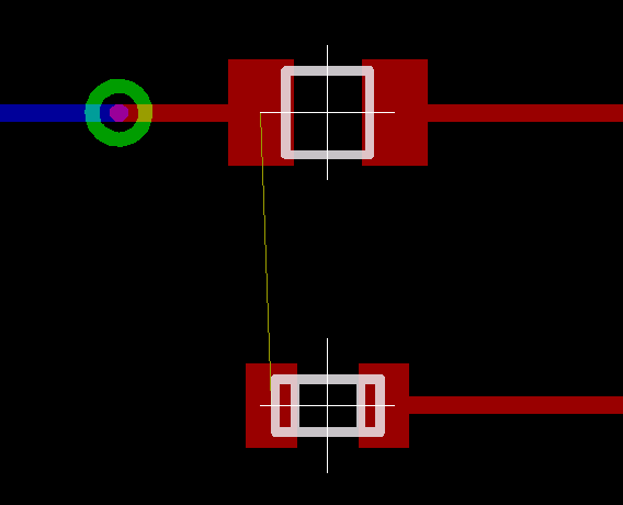
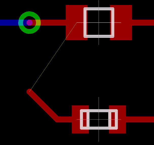
I wish to put signal in PCB over the via that is already exists. I won't create another via in the same place, but just use the one that has already been created. Please see the picture.
TNX

33_1172094044.JPG
 

eagle ripup error

Take a look at the pictures:
100_1172136670.gif

1) Same situation like yours

68_1172136701.gif

2) Route the signal (yellow wire) from the other side, which is not shown in your picture, toward via

53_1172136718.gif

3) End in the via. A small unrouted signal between via and pad will remain

12_1172136733.gif

4) Click on "Ratsnest" and the unrouted signal disappears
 

eagle cad tqfp

Hello everyone!!

I would like to know how we can convert the *.brd file to other format like *.jpeg, *.jpg, *.bmp and others without altering its dimensions so we can print the file anywhere we would like. I don't have any laser printer at home that i can use for printing but internet cafe's, in our place, do have this printers but the problem is they don't have this kind of software nor they will allow for installation.
 

eagle plcc library more pins

cloud said:
Hello everyone!!

I would like to know how we can convert the *.brd file to other format like *.jpeg, *.jpg, *.bmp and others without altering its dimensions so we can print the file anywhere we would like. I don't have any laser printer at home that i can use for printing but internet cafe's, in our place, do have this printers but the problem is they don't have this kind of software nor they will allow for installation.

from board window click CAM icon, select PS in device, scale 1, click file button and browse where you want to save the file (remember putting .ps as the extention for the file), select necessary layers, then process job.

now you have to find a software to convert postscript files to pdf, i use acrobat distiller.
 

eagle load error 291

I want to place 10 LEDs every 1cm - that is each LED will have a distance of 1 cm between them in a straight line.

How do I do this placement in EAGLE ?
 

eagle pcb dual led

hi all,
i have a problm ineagle that i can,t get green mask output for my pcb plz help me & thanks.
 

how do i put a +logo on my cad eagle

vsmGuy said:
I want to place 10 LEDs every 1cm - that is each LED will have a distance of 1 cm between them in a straight line.

How do I do this placement in EAGLE ?

use command grid, change unit to mm and size to 10
place the components and change everythig back.
 

library eagle zif

How can I flood fill the empty regions of the PCB with copper (after autorouting is done). This will expose less area to be etched and thus there will be a less consumption of etchant.
 

Status
Not open for further replies.

Part and Inventory Search

Welcome to EDABoard.com

Sponsor

Back
Top