Continue to Site

Welcome to EDAboard.com

Welcome to our site! EDAboard.com is an international Electronics Discussion Forum focused on EDA software, circuits, schematics, books, theory, papers, asic, pld, 8051, DSP, Network, RF, Analog Design, PCB, Service Manuals... and a whole lot more! To participate you need to register. Registration is free. Click here to register now.

If anybody need help in EAGLE, ask me in this POST !

Status
Not open for further replies.
i needed pic32 qfn foot print, part: PIC32MX534F064H
if anyone have it please attach here.

Have a on the Cadsoft site and type PIC32 in the search box. Even if the exact device isn't there, if there is one with the same package it can probably be easily edited. There may even be a suitable one in the standard Microchip library included with Eagle that you can edit.

Keith

- - - Updated - - -

- - - Updated - - -


This link is not working?

Go to http://www.cadsoftusa.com/downloads/ulps and type a keyword in for what you are looking for.

Keith
 

Hi,
I have a library for a BGA package 18*18. It has pads with pitch 1.27mm.
how can I change the pitch to 0.8mm without adjusting each pad manually?
Any kind of help is appreciated
Thanks.
 

This ULP may do what you want:

**broken link removed**

Other possible ones are:

**broken link removed**

Keith
 

This ULP may do what you want:

**broken link removed**

Other possible ones are:

**broken link removed**

Keith

Thanks for your reply.
I am getting error message " cannot open 'C:\Program Files\EAGLE 5.11.0\snap.scr' permission denied"
how to overcome this.
 

I don't know. I have just tried it and it works fine for me. You could contact the guy at Cadsoft who wrote it but it sounds more like a Windows problem - as if the file is still being shown as open. You could try closing Eagle and re-opening it and see if that helps.

Keith
 

I don't know. I have just tried it and it works fine for me. You could contact the guy at Cadsoft who wrote it but it sounds more like a Windows problem - as if the file is still being shown as open. You could try closing Eagle and re-opening it and see if that helps.

Keith

what exactly is the procedure for running ulp?
what i did-->opened a library for qfn 48 package-->ulp--> open 'snappad.ulp'-->then i got that error.
what should happen instead of showing error?
 

If you open the ULP with a text editor it will show you the instructions.

You run the ULP and it will create a script snap.scr. You then need to run that script (while still in the library) and the pads jump to the new location. I only tried it on a simple part but it worked.

Keith.
 

Re: eagle drill chart

Hi, Guys
i want to put some components in the bottom layer in my PCB (i use eagle software).
Can i make that just by mirror the component ? or there is another step beside that?
Are there a difference between placing the (DIP components or Resistors etc.) and the (SMD devices) in the bottom layer?

Thanks in advance,
Hz
 

There is nothing to prevent you from putting components on both sides of the PCB but it would be unusual to put DIP components on both sides. It is very common to put surface mount on both sides.

Keith
 

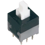
hey can anyone suggest me which footprint is suitable for this switch and how this switch is worked.
pcb design software eagle Push-Button-Switch.gif
 

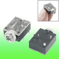
can anyone please tell me what this audio jack is called? and where i can find its footprint or datasheet?
 

audio jack, 3.5mm, stereo:
**broken link removed**
 
hi, i have a .sch file created in eagle. but my eagle version cant do simulation.spice mode.

is there any way for me to convert the .sch into something i can use to simulate my drawing elsewhere.tq
can anyone guide me through the process and clarify which simulator is compatible for me to use.

.sch > convert > anyfiletype > simulate at a free simulator site/software

pls.tq.
 

Have a look at Cadsoft's web site: **broken link removed** there is an LTspice interface now.

Keith
 

Does anyone can suggest a circuit to start with EAGLE? And any GOOD tutorial?

Regards.
 

In order to change a package, open Library, device you want to change, and package. Then, edit the pad there and save. CAUTION: From the nature of your question, I am guessing you are using the standard libraries. If you make the change as I just described, it will change the footprint for all devices that use that package.

So, I advise that you copy the device to a personal library, then make the change. You can name the package something unique and use it when you want that particular pad shape.

John
 

i wanted to change it in pcb file. my question is i placed a 18pin ic on eagle board . now i wanted to change the ic pad. in protel we can do that
by just simply clicking the pad. not in the library
 

Perhaps, if you told us the change you want to make, we might be able to give you better guidance.

John
 

Status
Not open for further replies.

Part and Inventory Search

Welcome to EDABoard.com

Sponsor

Back
Top