AllenD
Member level 5
Hi Team
Sorry for the long post.
I am using TSMC 65nm for an IC layout. I have finished the core and I am working on the input output pads. This tape out is for my research and not for mass production.
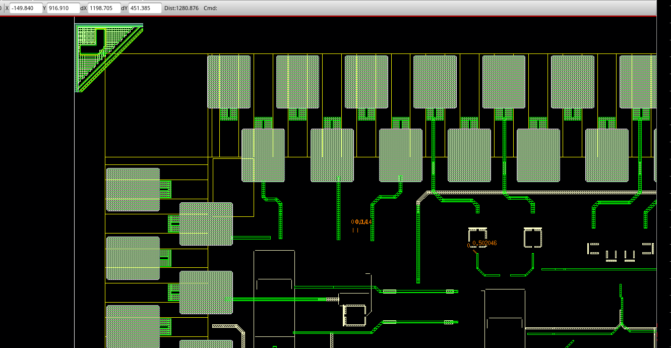
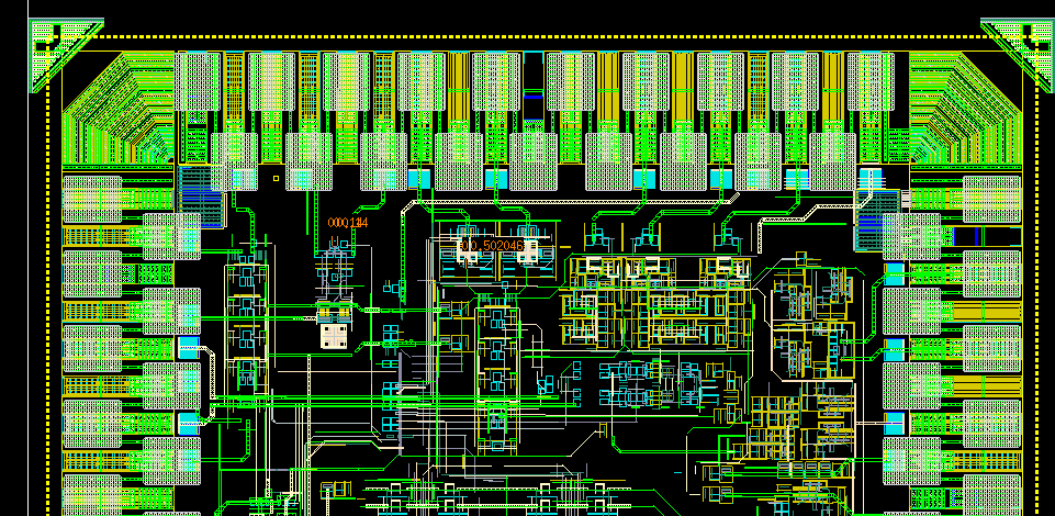
I had one tape out before. In that tapeout, I used 2 layer of pads (for more testing point and break out subcircuits) and using the ESD device provided by TSMC directly placed under the 2 layer of pads. Please see in the pictures.


The question are
1. I have heard some recommendation that I can just have the pads without the ESD bacause this tape out is just for research and to prove a new concept. I don't really care about the static charge protection that much, as long as one of the chips show me great performance, then the new idea is proven. Plus the ESD device would hurt the chip performance. In my design, the signal frequency is around 2.5GHz. Is there any broad estimation how bad would the ESD device hurt the chip performance?
2. If you agree I don't need the ESD under the pads, can I still use the 2 layer pads as in the above picture? Is there any draw backs with this type of pads layout? (not all pads need to be wirebonded at the same time. Some pads are for break out circuits only)
3. If I can get rid of ESD and using the 2 layer pads, what should I put under the pads in my layout? Should I leave them empty? Should manually add fillers? Or should I connect the fillers under the pad to ground? Should I connect these fillers with the fillerd (GND VDD mesh filers) in the core of my IC?
Thanks
Al
Sorry for the long post.
I am using TSMC 65nm for an IC layout. I have finished the core and I am working on the input output pads. This tape out is for my research and not for mass production.
I had one tape out before. In that tapeout, I used 2 layer of pads (for more testing point and break out subcircuits) and using the ESD device provided by TSMC directly placed under the 2 layer of pads. Please see in the pictures.
The question are
1. I have heard some recommendation that I can just have the pads without the ESD bacause this tape out is just for research and to prove a new concept. I don't really care about the static charge protection that much, as long as one of the chips show me great performance, then the new idea is proven. Plus the ESD device would hurt the chip performance. In my design, the signal frequency is around 2.5GHz. Is there any broad estimation how bad would the ESD device hurt the chip performance?
2. If you agree I don't need the ESD under the pads, can I still use the 2 layer pads as in the above picture? Is there any draw backs with this type of pads layout? (not all pads need to be wirebonded at the same time. Some pads are for break out circuits only)
3. If I can get rid of ESD and using the 2 layer pads, what should I put under the pads in my layout? Should I leave them empty? Should manually add fillers? Or should I connect the fillers under the pad to ground? Should I connect these fillers with the fillerd (GND VDD mesh filers) in the core of my IC?
Thanks
Al