ama_trig
Full Member level 2
- Joined
- Oct 9, 2009
- Messages
- 123
- Helped
- 20
- Reputation
- 40
- Reaction score
- 13
- Trophy points
- 1,298
- Location
- Where my hard drive lives!
- Activity points
- 2,100
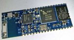
According to Aubtm-22 Document
**broken link removed**
1)If one sided pcb is to be used, Is vias needed ? if so, should I ground them? an how to implement it around the antenna?
2)If no plane is used under the module, is vias still a requirement?
3)copper area should be at least
20x15mm to maintain the best RF performance?? what does this mean ? where should be copper area implemented?
**broken link removed**
As with any RF devices, the AUBTM-22 requires careful attention to power supply and grounding
arrangements if its potential performance is to be realized.
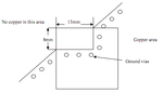
Fig.4 illustrates how PCB design around the antenna of AUBTM-22 should be made. The most
important thing is that there is no copper (ground plane or traces) underneath or in the close
proximity of the antenna.
It’s also very important to have grounding vias all the way in the border between ground plane
and free space, as illustrated with black and gray dots in figures above. This prevents the RF
signal for reflecting back to the PCB and signal lines over there.
Try to avoid any metal material near the antenna and keep at least 5mm away if it is inevitable.
A solid ground should be provide for AUBTM-22 and the copper area should be at least
20x15mm to maintain the best RF performance.
1)If one sided pcb is to be used, Is vias needed ? if so, should I ground them? an how to implement it around the antenna?
2)If no plane is used under the module, is vias still a requirement?
3)copper area should be at least
20x15mm to maintain the best RF performance?? what does this mean ? where should be copper area implemented?