NiedeLu
Junior Member level 3
Hi,
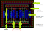
I have a problem concerning layout. My PMOS transistors are P-cells and are grouped depending on there function. Every group shares a NWELL and an isolation ring (PTAP and DNW). The NWELL should be taped to VDD near every transistor to get proper bulk connections. This is how i wanted to do it. But...
Now my problem:
If I draw an NWELL over a group of PMOS inside a iso-ring, ADS (Layout XL) says that there are shorts from the drains of the devices to the NWELL (VDD). I have no clue why this happens. There is an diode between D and NWELL (biased to VDD). Any suggestions on this? Tool issue? Do i miss something?
I'm not an experienced layout engineer..
Kindly asking for help. BR,
Lukas