Continue to Site

Welcome to EDAboard.com

Welcome to our site! EDAboard.com is an international Electronics Discussion Forum focused on EDA software, circuits, schematics, books, theory, papers, asic, pld, 8051, DSP, Network, RF, Analog Design, PCB, Service Manuals... and a whole lot more! To participate you need to register. Registration is free. Click here to register now.

CMOS dc -dc convertor design M.E project

Status
Not open for further replies.
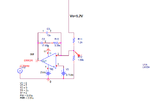
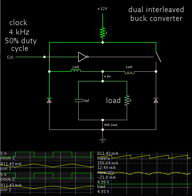
Often convergence errors occur when I have 3-terminal devices, and I power them from one supply voltage, yet drive the base/gate from a different voltage. In real life it is not necessarily an error. But the simulator gets confused.

In particular, your buck converter has a 12V supply. The mosfet gates are driven by 20V. There's a chance this causes the error. It would be easier if the simulator would tell us, wouldn't it?

Another possibility: mosfet M2 is N-type. Its gate is referenced to the source terminal. For it to turn on, it needs to see a definite lower volt level at the source terminal. However there are components intervening in the path to ground.

Furthermore when it turns on, it conducts 12V to the node below it, and the node goes to almost 12V. To solve this with real hardware we drive the gate with 20V... But how the simulator interprets it, only the simulator knows.

It may help if you use a P-mos for the high side.


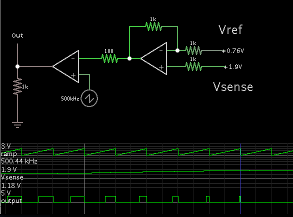
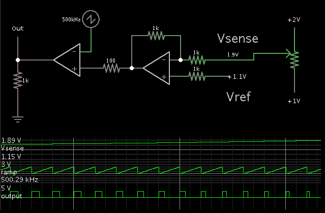
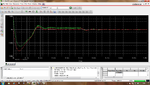
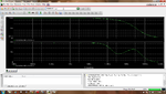
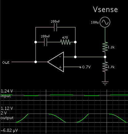
i wanted to know how to connect the output of the comparator lt1016 to M2 whose gate is not referenced to ground but referenced to source, while the output of the comparator is referenced to ground i think. I am attching the schematic again also i have attached the output of the pwm comparator and i think the pwm is not correct i.e when the error is more the pulse width should be more, but here it is less for more error and becomes more for small error.I am not getting where to make the changes for the pwm, tried changing the ramp amplitude,but that may be trial and error.Are there any design equations for this ?
 

Attachments

  • SCHEMATIC1 _ PAGE1.pdf
    16.3 KB · Views: 50
  • par.pdf
    33.8 KB · Views: 46

when the error is more the pulse width should be more, but here it is less for more error and becomes more for small error.I am not getting where to make the changes for the pwm, tried changing the ramp amplitude,but that may be trial and error.Are there any design equations for this ?

It will work properly if you apply your reference voltage V5 to the inverting input, and apply your sense voltage to the non-inverting input. You may need to adjust volt levels, gain, etc.

Screenshot:

 
It will work properly if you apply your reference voltage V5 to the inverting input, and apply your sense voltage to the non-inverting input. You may need to adjust volt levels, gain, etc.

Screenshot:


i tried the way you told.But i did not get why that change of sense voltage application to non inverting input matters. Basically it should produce a inverted error voltage as compared to the previous case i.e connecting it to the inverting input.I designed a PI compensator for my design also(as can be) seen in the schematic attached. I now need gate drivers for my design or can i do without gate drivers, any simple way to do ? I also cant be sure that my ckt works until i complete the loop. Please help
 

Attachments

  • SCHEMATIC1 _ PAGE1.pdf
    16.2 KB · Views: 57

i tried the way you told.But i did not get why that change of sense voltage application to non inverting input matters.

To be honest, I went on the old saying: 'If it doesn't work the way you hooked it up, then try reversing the connection.'

The inverting input is tricky that way.

An alternate solution is to switch the inputs at your second op amp instead. What you have then might agree better with your intuitive sense of how the two op amps cooperate.

Screenshot:


I now need gate drivers for my design or can i do without gate drivers, any simple way to do ?

The big question mark is whether your mosfets will turn on fully in response to a 5V pulse. If they will, then you don't need to step it up.


The big question mark is whether your mosfets will turn on fully in response to a 5V pulse. If they will, then you don't need to step it up.

Ya that i have noticed the mosfets wont give proper unless the gate is at 12+threshold.That is why i need to shift the pwm from the 4V to about 15
I am searching for something to do that
 

To be honest, I went on the old saying: 'If it doesn't work the way you hooked it up, then try reversing the connection.'

The inverting input is tricky that way.

An alternate solution is to switch the inputs at your second op amp instead. What you have then might agree better with your intuitive sense of how the two op amps cooperate.

Screenshot:


The big question mark is whether your mosfets will turn on fully in response to a 5V pulse. If they will, then you don't need to step it up.

I have got my ckt working and it seems to regulate properly.But i have a few doubts to clear.I am attaching schematic and some outputs
When i start the converter i see the voltage drop from 8 volts, goes -ve and then stabilizes to 1.18V, but previously it directly went from 0 to 1.18 Why this change now ?
Also in the image named schematic you can see one of the pwm below zero(-ve) which i think should have been above zero just the complimented version of the other.But with this even my converter regulates. This must not be proper,yes?
I also need to introduce dead time in the pwm and require something that provides me phase shift
i had read about dead time using a resistor and diode but did not get the concept properly.Needed a diagram if any or an alternative way.Dont want to introduce unwanted delays in the feedback loop
Also need phase shifting ckt of multiphase operation.Please help
 

Attachments

  • SCHEMATIC1 _ PAGE1.pdf
    16.9 KB · Views: 51
  • PWM_outputs.png
    PWM_outputs.png
    192.3 KB · Views: 68
  • output.png
    output.png
    161.7 KB · Views: 56
  • capacitor_and_inductor _current.png
    capacitor_and_inductor _current.png
    171.7 KB · Views: 65

Needed help to find the bode plot of the compensator in the figure.I designed it according to one application note from international rectifier.
I wanted to change the ESR of the capacitor from 10m to 5m and so on and check the effects on transient response.But when i did that found my output started to become unstable. So i thought the compensator is not stable. so need help regarding this as i am not well versed in control theory. Please help
 

Attachments

  • SCHEMATIC11 _ PAGE1.pdf
    17.1 KB · Views: 49

I see your latest posts but I'm afraid my knowledge is meager in the face of the problems you report.

Design is easier when one of the switches is a diode, but things get tricky when doing synchronous mode. I have a simulation running where the output stays a fraction of a volt negative due to the capacitor discharging back up through the coil at odd times when it gets a chance. Can't figure out why.

Another of my synchronous mode simulations looks okay and I can't figure out what I'm doing right.

Post 46: The green scope trace shows output V surging briefly on startup. This is typical. If your load cannot tolerate the overvoltage then you may need to delay connecting it until after output settles.
 
Hello,
I have designed this pi controller according to the pdf that i have attached
These are my specifications Vin=12V
vout=1.2V
Iout=12A
Vripple=2% of Vout=24mV
iripple= 20% of iout= 2.4A
Fs=500K
L=900nH
C=2.25mF to handle a step of 12A
D=vout/Vin =0.1
Rload=Vout/Iload=1.2/12=0.1
ESR of capacitor is 10m
The problem is my circuit regulates well for these values,but when i make variations the output starts oscillating
I have also attached the bode plot of the same, i dont have any idea if the bode plots are correct or not.
Please someone can suggest me any refernce where i can actually understand what i should do will be very helpful
 

Attachments

  • very_imp.pdf
    1.3 MB · Views: 71
  • error_amplifier.png
    error_amplifier.png
    12.1 KB · Views: 59
  • gain_phase_plot.png
    gain_phase_plot.png
    163.5 KB · Views: 58

The problem is my circuit regulates well for these values,but when i make variations the output starts oscillating

I see this is similar to Fig. 5 on page 8 of the application note. The type II compensator.

I'm running a simulation. The error amplifier works, although the capacitor feedback seems to create exaggerated swing in the output.

Screenshot:

6458567900_1358881715.png


Vsense varies only a total of 0.12 V. Yet the output swings from one supply rail to the other.

I tried reducing the gain, by increasing the cap values and decreasing the resistor.

I believe it will help if you experiment with these values, until you get the output to respond smoothly rather than go into oscillation.
 

This is IRF150 power mosfet subcircuit file
*-------------------------------------------------------------------------------
* Library of MOSFET model parameters (for "power" MOSFET devices)
*
* This is a reduced version of PSpice's power MOSFET model library.
* You are welcome to make as many copies of it as you find convenient.
*
* The parameters in this model library were derived from the data sheets for
* each part. Each part was characterized using the Parts option.
* Device can also be characterized without Parts as follows:
* LEVEL Set to 3 (short-channel device).
* TOX Determined from gate ratings.
* L, LD, W, WD Assume L=2u. Calculate from input capacitance.
* XJ, NSUB Assume usual technology.
* IS, RD, RB Determined from "source-drain diode forward voltage"
* specification or curve (Idr vs. Vsd).
* RS Determine from Rds(on) specification.
* RDS Calculated from Idss specification or curves.
* VTO, UO, THETA Determined from "output characteristics" curve family
* (Ids vs. Vds, stepped Vgs).
* ETA, VMAX, CBS Set for null effect.
* CBD, PB, MJ Determined from "capacitance vs. Vds" curves.
* RG Calculate from rise/fall time specification or curves.
* CGSO, CGDO Determined from gate-charge, turn-on/off delay and
* rise time specifications.
*
* NOTE: when specifying the instance of a device in your circuit file:
*
* BE SURE to have the source and bulk nodes connected together, as this
* is the way the real device is constructed.
*
* DO NOT include values for L, W, AD, AS, PD, PS, NRD, or NDS.
* The PSpice default values for these parameters are taken into account
* in the library model statements. Of course, you should NOT reset
* the default values using the .OPTIONS statement, either.
*
* Example use: M17 15 23 7 7 IRF150
*
* - - - - - - - - - - - - - - - - - - - - - - - - - - - - - - - - - - - - - -
*
* The "power" MOSFET device models benefit from relatively complete specifi-
* cation of static and dynamic characteristics by their manufacturers. The
* following effects are modeled:
* - DC transfer curves in forward operation,
* - gate drive characteristics and switching delay,
* - "on" resistance,
* - reverse-mode "body-diode" operation.
*
* The factors not modeled include:
* - maximum ratings (eg. high-voltage breakdown),
* - safe operating area (eg. power dissipation),
* - latch-up,
* - noise.
*
* For high-current switching applications, we advise that you include
* series inductance elements, for the source and drain, in your circuit file.
* In doing so, voltage spikes due to di/dt will be modeled. According to the
* 1985 International Rectifier databook, the following case styles have lead
* inductance values of:
* TO-204 (modified TO-3) source = 12.5nH drain = 5.0nH
* TO-220 source = 7.5nH drain = 3.5-4.5nH
* - - - - - - - - - - - - - - - - - - - - - - - - - - - - - - - - - - - - - -
*
.model IRF150 NMOS(Level=3 Gamma=0 Delta=0 Eta=0 Theta=0 Kappa=0 Vmax=0 Xj=0
+ Tox=100n Uo=600 Phi=.6 Rs=1.624m Kp=20.53u W=.3 L=2u Vto=2.831
+ Rd=1.031m Rds=444.4K Cbd=3.229n Pb=.8 Mj=.5 Fc=.5 Cgso=9.027n
+ Cgdo=1.679n Rg=13.89 Is=194E-18 N=1 Tt=288n)
* Int'l Rectifier pid=IRFC150 case=TO3
* 88-08-25 bam creation

Can someone tell me where is the on resistance of this Mosfet stated in this file
In the data sheet it is given as 0.055
 

I read on a paper that for say a 12/1.5V, 20A voltage regulator module if you use a single stage synchronous buck you will require a large output capacitor which will eat up too much space on the motherboard and make the design impractical. so the solution to this is use multiphase synchronous buck which will reduce the size of the output capacitance
My question is:- For saving the board space if you are using a multiphase VRM, it will have more no of MOSFETs as compared to the single phase, wont it again increase the size
Isnt the reduction of capacitor size cancelled by the increased no of MOSFETs ?

Ah, you're thinking ahead. A good quality to have.

There is also the option of using interleaved converters (2 or more). This will involve an additional coil and mosfet and driver circuitry.

Each topology has its advantages and disadvantages. As you examine these, you will eliminate this or that method.

Whichever method you choose, it will be a tradeoff between the ideal and the possible.

To answer your question, besides considering board space, there is the high current (20A or more) that your converter will handle. If the simulator is correct, your smoothing capacitor must carry several amps back and forth at 500 kHz. I believe you will need more than one capacitor. They can be rated for 3 or 4 or 5 V, so they will not take up much space. However the volt level may surge on power-up, so I could be wrong about using such a low volt rating.
 
Another thing, to reduce current ripple higher inductance is needed. To determine inductance i use the relation (Vin-Vo)D/(Fs*Iripple)
Iripple is chosen as 20% of load current.What changes occur in the design when the load changes ?
I am confused by this thing that if my load current increases then the 20% ripple also increases and the ripple has a inverse relation to L
So higher load means higher ripple and lower L value which contradicts higher ripple requires higher inductance to reduce it
Please help me with this
 

What changes occur in the design when the load changes ?

Greater load draws down the capacitor charge more rapidly during switch-Off time. This causes an increase in ripple.
To remedy this you can increase the capacitor or raise the frequency.

Increasing the Henry value makes coil current ramp up or down more gently. If frequency stays the same, you'll get less ripple. If the switch is controlled by hysteresis the frequency will get slower and ripple will stay the same.

To get a grasp on how all these interact, it helped me to spend a few hours with the interactive animated simulator.
 
Transient response of a DC-DC converter depends on different things like control, filter parasitics and so on. Can someone elaborate the effects of input voltage and output voltage on the transient response
 

In a mutiphase buck converter what is the need of giving phase shifted signals to the high side MOSFETS ?
 

In a mutiphase buck converter what is the need of giving phase shifted signals to the high side MOSFETS ?

The control signals are staggered, in order to switch the coils alternately on and off. The load is split between two converters.

That way the supply does not need to provide a single high peak, but two lesser peaks. This method is useful if the supply current is limited due to internal impedance (portrayed by a 3 ohm resistor in the screenshot below).

Another benefit is reduced ripple at the load. Hence the smoothing capacitor can be a lower value.


"Generic" switches are used to represent transistors/mosfets at the high side.
 

That way the supply does not need to provide a single high peak, but two lesser peaks. This method is useful if the supply current is limited due to internal impedance (portrayed by a 3 ohm resistor in the screenshot below).

I did not get what a single high peak means.Please elaborate on that.
Also what is the impact of input and output voltage on transient response of a buck converter ?
 

I did not get what a single high peak means.Please elaborate on that.

It was a strange choice of words. I meant the high-peaking waveform of a single converter. With interleaving that high current waveform is divided down to two lesser peaks, staggered.

Also what is the impact of input and output voltage on transient response of a buck converter ?

A non-regulated output will take a few cycles to settle to a new value. If you lighten the load suddenly, the output volt level will soar for a while. This may be bad for the load.

Sometimes the coil and capacitor values combine in a way that creates a resonant loop. Then the output level might wander above and below the new value for several cycles.

Not sure if this is what you were asking about.
 

Status
Not open for further replies.

Part and Inventory Search

Welcome to EDABoard.com

Sponsor

Back
Top