Continue to Site

Welcome to EDAboard.com

Welcome to our site! EDAboard.com is an international Electronics Discussion Forum focused on EDA software, circuits, schematics, books, theory, papers, asic, pld, 8051, DSP, Network, RF, Analog Design, PCB, Service Manuals... and a whole lot more! To participate you need to register. Registration is free. Click here to register now.

CMOS dc -dc convertor design M.E project

Status
Not open for further replies.

vinayakdabholkar

Advanced Member level 4
Joined
Nov 29, 2009
Messages
114
Helped
0
Reputation
0
Reaction score
0
Trophy points
1,296
Location
goa
Activity points
2,195
Help needed--CMOS dc -dc convertor design M.E project

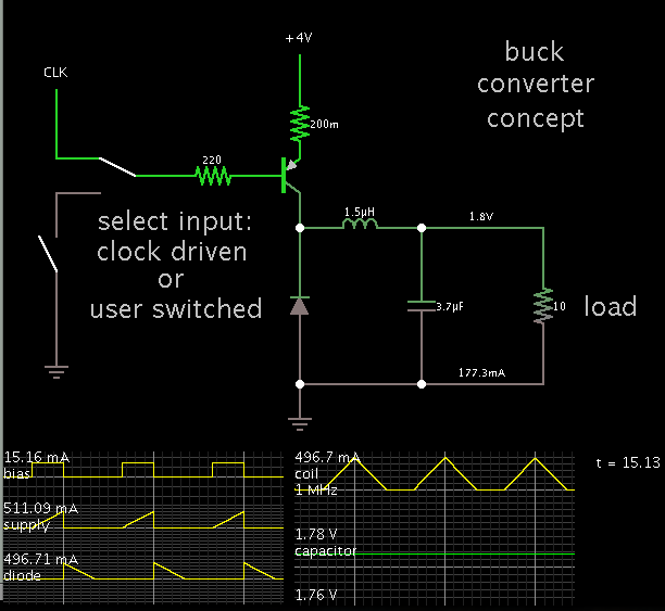
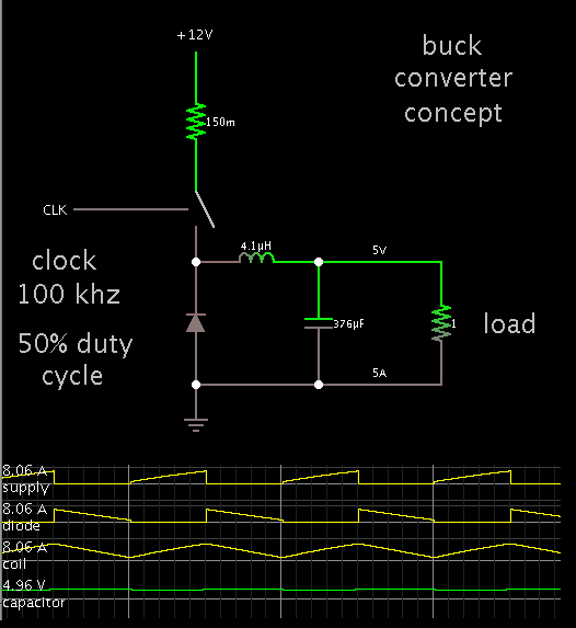
Hello , i am interested in designing a cmos dc- dc convertor for my project.Its titled "Design and analysis of interleaved multiphase dc-dc convertors"
i want to start with design of a synchronous buck and then compare it against an multiphase interleaved design
so what technology has to be used to design this and why ? e.g nanometer, micrometer
what should i look into before starting or how should i go about it ?
i am thinking about using ngspice to simulate the ckts
any reference material if suggested would be great help

Thank you
 

A good article is at the link below. It has a few pages on interleaved multiphase type.

**broken link removed**

Are you acquainted with the single asynchronous buck converter? In simulation or real-life?
 
i am not acquainted with a asynchronous buck in real life nor i have done any simulations yet.
ill check the link .
Thank you very much.
 

i finally read the manual and found it very useful. i now wanted to start simulating the circuits. I wanted to know which is the best software to do so. I was thinking of using matlab. Also i wanted to know what are the issues in present day dc/dc buck converters which are used.

Thank you
 

i finally read the manual and found it very useful. i now wanted to start simulating the circuits. I wanted to know which is the best software to do so. I was thinking of using matlab. Also i wanted to know what are the issues in present day dc/dc buck converters which are used.

I have found that an interactive animated simulator is invaluable, for understanding difficult concepts about how certain circuits operate.

It helped me to learn about switched coil converters.

Since the coil is at the center of action, it is important to know how current builds and decays in the coil.

I constructed a buck converter using the simulator at the falstad.com website. The cycle can be clock controlled, or user controlled.

Below is a link which will open the website, load my simulation, and run it on your computer. (Click Allow to permit the connection.)

https://tinyurl.com/94nlzsu

It is asynchronous rather than synchronous.

It has two switches you can click. One switch selects between (1) a clock drive or (2) user clicks. You click on the second switch to begin the power cycle through the coil. Then let up the switch to watch the output cycle.

You can alter values at will. Right-click on a component to bring up an edit window.
 
Thanks.
Will simulate the circuits and thought of doing loss modelling of DC/DC buck converter using matlab.
 

can someone please help me with this converter in simulink. I am not understanding how to get this pwm operating.
this is a buck converter intended for 1Mhz operation
capacitor 3.75u
inductor 1.5u
input voltage 4V
expected output 7.5V
 

Attachments

  • buck.rar
    8.5 KB · Views: 127

can someone please help me with this converter in simulink. I am not understanding how to get this pwm operating.
this is a buck converter intended for 1Mhz operation
capacitor 3.75u
inductor 1.5u
input voltage 4V
expected output 7.5V

A buck converter is used to step down the supply voltage.

To step up, the type to use is a boost or buck-boost.

You can use the same component values.
 

sorry for the mistake. The expected output is not 7.5 its 1.75V
I was not getting the pwm to work for the Mosfet switches. Wanted to know about the compensation network needed for the converter. How to go about designing one.
Thanks
 

That's pretty funny. To me at least. Because the last DC-DC
I designed took us 3 years and half a dozen spins to get all
wrung out, and I was only responsible for some pieces of it -
team of three, all very experienced.

So it ought to fit nicely within your semeter of time and your
available level of effort.

Your technology will be driven primarily by your VIN supply
and how heroic you want to be in accommodating it (natural
device, or some stack-of-N scheme with appropriate isolation
technology). Speed is seldom the concern since users have
a hard time getting passives that support high frequency
operation anyhow.
 
sorry for the mistake. The expected output is not 7.5 its 1.75V
I was not getting the pwm to work for the Mosfet switches. Wanted to know about the compensation network needed for the converter. How to go about designing one.
Thanks

To get a grasp as to the interaction beween operating frequency, duty cycle, and output volt level at the load...

it helps to have an animated interactive simulator. (It helped me.)

Screenshot:


The link below will open falstad.com/circuit, load my schematic, and run it on your computer. (Click Allow to load the Java applet.)

https://tinyurl.com/cp4akee

Click on the switch at left to begin the switch-'On' cycle. Let up to see the switch-'Off' cycle.

The idea is to click it at the correct rate, so that you get 1MHz, and 1.75V on the load. (I used an arbitrary load resistance.)

The coil is the center of action. Watch the waveform through the coil.
 
- - - Updated - - -

To get a grasp as to the interaction beween operating frequency, duty cycle, and output volt level at the load...

it helps to have an animated interactive simulator. (It helped me.)

Screenshot:


The link below will open falstad.com/circuit, load my schematic, and run it on your computer. (Click Allow to load the Java applet.)

https://tinyurl.com/cp4akee

Click on the switch at left to begin the switch-'On' cycle. Let up to see the switch-'Off' cycle.

The idea is to click it at the correct rate, so that you get 1MHz, and 1.75V on the load. (I used an arbitrary load resistance.)

The coil is the center of action. Watch the waveform through the coil.


Checked the animation.
I have understood the concept. Need to model with either simulink/pspice . I have decided simulink and even started with that. So i have the basic synchronous buck done(open loop) . Now need info regarding the feedback to use.
what will determine the transient response (the settling time of the output for load variations) of the converter. And for it to be practical what should i look into. Reference material is needed
Thanks
 
Last edited:

can you help me with this equation diL/dt=1/L(vg*D-Vo) this is the equation for inductor current in a buck converter. Vg is the input, D duty cycle and Vo the output
also i have another equation iL= 1/L(Vg-Vo)t +iL(0) this is obtained after integrating. The peak inductor current occurs at t=DT .The first equation doesnt have this time thing when implemented directly , but after integrating the t is introduced (0<t<DT and DT<t<T).How to implement this in simulink and find the peak nductor current by setting the time

- - - Updated - - -

That's pretty funny. To me at least. Because the last DC-DC
I designed took us 3 years and half a dozen spins to get all
wrung out, and I was only responsible for some pieces of it -
team of three, all very experienced.

So it ought to fit nicely within your semeter of time and your
available level of effort.

Your technology will be driven primarily by your VIN supply
and how heroic you want to be in accommodating it (natural
device, or some stack-of-N scheme with appropriate isolation
technology). Speed is seldom the concern since users have
a hard time getting passives that support high frequency
operation anyhow.

True. The project idea was initially really wague. I did not had any idea of the thing.Nor do i have the skiils or tools to design such a converter nor my semester system gives me the time. I want to design a multiphase buck with improved transient response.
Thanks for your reply
 

Please someone help me with this ckt. Expected output is 5V . why it is not working ?

- - - Updated - - -

but it works if i directly connect as in the second pdf
 

Attachments

  • SCHEMATIC1 _ PAGE1.pdf
    9.9 KB · Views: 125
  • SCHEMATIC1 _ PAGE1.pdf
    9.5 KB · Views: 115
Last edited:

Please someone help me with this ckt. Expected output is 5V . why it is not working ?

- - - Updated - - -

but it works if i directly connect as in the second pdf

Here is my simulation of your first schematic. It appears to work properly. Its operation is practically identical to your second one.


If I were to offer a bold opinion, I would suggest your wiring at the controller IC is incorrect.

There is also the usual advice regarding diodes... a fast recovery type is recommended if your frequency is higher than a few kHz.
 
I] I am not able to understand this working.In the first image(named T1) it is said energy stored in C1 is discharged to L1 via Q1.
why dosent the energy in C1 flow directly to L7 ?
Also it is said C3 transfers its energy to L5 since it has no other path for its energy to discharge . But it is connected to ground, cant it discharge to ground ?
II] in the second image(T2) how is the current flowing through L3-L6-L8.

can some one explain the working of this please


III] This is my synchronous buck converter. It is designed to give 5V output , but it gives 4V. I tried varying the duty cycle. But i found out it increases just above 4 and further increasing the duty output starts reducing.
What design changes should be made as i have designed the components for 100K freqency
 

Attachments

  • T1.png
    T1.png
    234.8 KB · Views: 120
  • T2.png
    T2.png
    300.9 KB · Views: 132
  • SCHEMATIC1111 _ PAGE1.pdf
    13.4 KB · Views: 120
Last edited:

I] I am not able to understand this working.In the first image(named T1) it is said energy stored in C1 is discharged to L1 via Q1.
why dosent the energy in C1 flow directly to L7 ?
Also it is said C3 transfers its energy to L5 since it has no other path for its energy to discharge . But it is connected to ground, cant it discharge to ground ?
II] in the second image(T2) how is the current flowing through L3-L6-L8.

can some one explain the working of this please

Wow, there sure is a lot going on in this schematic.

Your questions are reasonable. I am trying a simulation which shows the interaction simultaneously in all wires, by means of current flow.

I am getting resonant action among the coils and capacitors. Sometimes current flows back into the supply. I don't believe that's supposed to happen. The purpose is to make the incoming supply constant, and to reduce ripple on the incoming supply.

To make any progress, I will need to get the values adjusted right, and get the switching sequence right.
 
These are the schematic of my buck converter and the inductor current. As can be seen the insuctor current is less than 0.
In which mode is it operating CCM or DCM ?
For CCM inductor current goes minimum to 0 but here it is less than 0
whereas for DCM it has to go to zero and remain there for last part of the cycle , but in the diagram the current is continuous.Is the ckt wrong ?
 

Attachments

  • SCHEMATIC1 _ PAGE1_upload.pdf
    13.4 KB · Views: 142
  • upload.pdf
    36 KB · Views: 114

Status
Not open for further replies.

Part and Inventory Search

Welcome to EDABoard.com

Sponsor

Back
Top