Continue to Site

Welcome to EDAboard.com

Welcome to our site! EDAboard.com is an international Electronics Discussion Forum focused on EDA software, circuits, schematics, books, theory, papers, asic, pld, 8051, DSP, Network, RF, Analog Design, PCB, Service Manuals... and a whole lot more! To participate you need to register. Registration is free. Click here to register now.

BJT ESD failure, anyone has experience with that?

Status
Not open for further replies.

cmosbjt

Full Member level 5
Joined
Apr 25, 2004
Messages
250
Helped
10
Reputation
20
Reaction score
2
Trophy points
1,298
Location
USA
Activity points
2,293
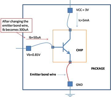
Hi, I have trouble using a bipolar transistor without ESD protection. As shown in the picture. When the open face package is built, the transistor works fine.

The collector current: Ic = 5mA,
The base current: Ib = 50 uA,
The base voltage: Vb = 0.85V

As you know by changing the emitter downbond, we can adjust the RF gain. So we change the emitter bond wire once in a while. But that cause most the trouble. After changing the emitter bond wire, the BJT draws a lot of base current in order to maintain the Ic and Vb:

The collector current: Ic = 5mA,
The base current: Ib = 300 uA,
The base voltage: Vb = 0.85V

So I believe the device is damaged.

My questions are:

1. Does anyone has similar experience as this one?
2. Do you know what is the mechanism of the damage? Any reference articals?
3. Is there any failure analysis procedure I can do to confirm/verify the damage?
4. How do you handle this unprotected device if changing the bondwire is neccesary?

Thanks

32_1202677473.jpg
 

from your decription the transistor doesn't look dead.
I think this may caused by some parasitic devices which leakage the other 250uA.
 

If your bond pads are on top of the device junctions it sounds like you are damaging the E/B juction by changing the bond wire. The stress of pulling the bond wire off or the stress of rebonding a new wire or both could be damaging them.
 

Troy said:
If your bond pads are on top of the device junctions it sounds like you are damaging the E/B juction by changing the bond wire. The stress of pulling the bond wire off or the stress of rebonding a new wire or both could be damaging them.
No, the bond pad is far away from the device. And BTW, the bond wire is changed by our very professional assembly group. They have 30 years experience.

Added after 2 minutes:

extraord said:
from your decription the transistor doesn't look dead.
I think this may caused by some parasitic devices which leakage the other 250uA.
Such as ???.
 

Was this transistor tested on MM,CDM and HBM and thus it corresponds to this behavior?
 

Is it possible to post the Gummel curve for the device before and after (damage)? From the Gummel curve, you can tell if your e-b junction has high leakage or if your CB or CE junctions are damaged.

Any chance of the emitter potential being pulled higher than the base during the bonding process or post-bonding process?
 

It's been my experience that you cannot change a bondwire. Removing/rebonding often damages the silicon under the bondpad, which is usually doped N to act as a simple ESD device. Damaging this junction makes it leaky.

The failure analysis you should do is to curve-trace the BE juntion. If it was ESD zap, then the BE has been damaged as if it were a zener diode.

But I think you may need to cut the metal trace from emitter to bondpad on a damaged device and make sure the leakage is not directly through the bondpad.

And are you positively sure that with the new bondwire inductace, your device is not simply oscillating? Even emitter follower can oscillate if there is feedback through the EB capacitance.
 

ni hui shou yingwen ma?

because this board is in yingwen. so use it.
 

Possibly it is damaged by ESD stress on BE junction.
What's the size for your device?
If it is big enough, maybe you can try to short B and C during E bonding changing. It will hehave as ESD protection for itself.
 

Is it possible from the temperature variation?
for example, the different package or bonding changes the thermal conditions and ...
 

Status
Not open for further replies.

Part and Inventory Search

Welcome to EDABoard.com

Sponsor

Back
Top