Continue to Site

Welcome to EDAboard.com

Welcome to our site! EDAboard.com is an international Electronics Discussion Forum focused on EDA software, circuits, schematics, books, theory, papers, asic, pld, 8051, DSP, Network, RF, Analog Design, PCB, Service Manuals... and a whole lot more! To participate you need to register. Registration is free. Click here to register now.

[Moved]Sharing ADC and GPIO PADs that supports 5V tolerant

fredhdx573

Newbie
Joined
Sep 29, 2023
Messages
4
Helped
0
Reputation
0
Reaction score
0
Trophy points
1
Activity points
49
Hello everyone,

I have a question that I would like to share with you:

I am currently working on a project where I want to share the input PAD of an ADC with the GPIO's PAD. The main purpose behind this is to save costs. The GPIO PAD supports 5V tolerance, while the ADC only allows a maximum input voltage of 3.6V. I have implemented a switch (transmission gate) between the ADC and the PAD, which allows me to turn off the ADC when it is not in use. However, I have a concern regarding the situation where the PAD voltage is 5V, as it could potentially conduct through the PMOS of the switch and damage the ADC. Could someone please guide me on how to address this issue?
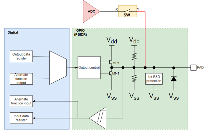
1696931868918.png


Thank you all for your assistance.

Best regards,
 
Hi,
Could someone please guide me on how to address this issue?
First you need to verify that the "absolute maximum input voltage" of the ADC really is just 3.6V.
Often useres here misinterprete the "decodable input voltage range" as maximum allowed.

But if the ADC input is limited to 3.6V, then - simply speaking - you have to accept this specification.
* Either by using a resistive voltage divider,
* or a comparator that "disables" the switch on overvoltage
* or by using an ADC with 5V tolerant input
* or .. any other solution

Klaus
 
Thanks FvM and Klaus for your feedback.

Hi FvM,
Yes, my question is related to IC design.
Do you have any idea to design a transmission gate that can protect 5V input? As my investigation, only NMOS-gate can protect 5V, while PMOS cannot. However, only using NMOS will limit the input voltage lower than VDDA-Vth

1696990919835.png


Hi Klaus,

Yes, the ADC can only accept input voltage < 3.6V. My design target is that when the ADC is active, the transmission gate is ON, and the input PAD will be limited at <3.6V. However, when the ADC is disabled, the transmission gate is OFF, the PAD is used for GPIO input can be up to 5V, and the transmission gate can protect the ADC from 5V damage.

I'm not sure how to design the transmission gate like this. Do you have any ideas?
 
The problem may be that the "5V" pads are not really using
5V devices so a front end blocking / pass FET and pullup
do the job. But this style makes the voltages inboard of
the special front end, 0 - VDD (any overrange is clipped).

You should be clear about the ADC input range, what "box"
you are in, whether (say) you want a 3/4 divider resistor
network (DC) or capacitor network (AC) to scale to range,
can you stand the distortion / delay / BW limit that a protection
network may impose, etc. as you try to choose.
 
Thank you, dick_freebird, for sharing your opinion.

However, I am still seeking ideas on designing a switch that effectively protect ADC from a 5V input. If anyone has any suggestions or insights, I would greatly appreciate your input.

Best Regards,
Fred
 
You might look at analog multiplexers, there is a subset which offers
"overvoltage protection" of various forms (high-Z, hard limited, etc.).

Now any CMOS switch, not of that kind, will tend to clamp signal at
VDD+Vf and that is same as the ADC ((but more stout, if it's a
piece-part, perhaps) if you co-power it.

Surely the exact Vf and stiffness will vary. You might do a little bench
I-V testing of such candidates at your imagined threat-voltage,
threat-current levels and find one that's best for that seldom-
advertised attribute.
 

LaTeX Commands Quick-Menu:

Part and Inventory Search

Welcome to EDABoard.com

Sponsor

Back
Top