Continue to Site

Welcome to EDAboard.com

Welcome to our site! EDAboard.com is an international Electronics Discussion Forum focused on EDA software, circuits, schematics, books, theory, papers, asic, pld, 8051, DSP, Network, RF, Analog Design, PCB, Service Manuals... and a whole lot more! To participate you need to register. Registration is free. Click here to register now.

Why pcb wires looks like loops?

Status
Not open for further replies.

yikes

Newbie level 4
Joined
Mar 2, 2012
Messages
6
Helped
0
Reputation
0
Reaction score
0
Trophy points
1,281
Location
Spain
Activity points
1,349
Hi all,

I am a student trying to learn as much as posible about electronics. This is my first post in edaboard.
Some time ago, a friend gave me a TFT controller board from Techtoys. It is a SSD1963 controller board.
Since i received it i was wondering why the designer of the board made some traces (a lot of traces) that looks like loops or similar.
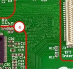
tft.jpg

above there is a screen capture from the manual that shows the traces. They are the RGB and other signals that goes from the controller chip to the TFT connector.
What is the reason that these traces was made like loops? I was looking for information (in google) about this without success.

Thanks.
 

I think this can be some inductor.

But this looks like very creapy. This looks like as they wanted to occupy the space so something else that cannot be placed there.
 
Last edited:

Dear yikes and Dear tpetar
Hi
I'm agree with tpetar .
Those are inductors ( like and RFC ) to block high frequency , AC signal . and at high frequencies we can design our inductors with lines of PCB ( because the inductors that we need at those frequencies , can't exceed from some hundred or some , nano henry.
Best Things
Goldsmith
 

Also, people do that to try to keep trace lengths the same (e.g. if you had a clock with balanced output, then you would want the delay to be exactly the same).
 

Now it is more clear to me.
Very thank you all for your answers.
 

this could be serpentine routing to match length the traces to the connector.
 

Not inductors. Length matching is the correct reason for such a routing scheme.
This is usually done with bus signals that have to reach their Rx point at the same time.
Think of the signals as cars and on the PCB traces as roads.
Sometimes, all your cars must arrive at the destination at the same time (as with a high speed memory bus).
The propogation speed of the signals you see is the same and they leave the Tx end at the same moment - so the only way to ensure they all reach the Rx point at the same time is make them travel the same distance.
 
  • Like
Reactions: yikes

    yikes

    Points: 2
    Helpful Answer Positive Rating
Dear shaiko
Hi
But , i saw , many circuit's with line strip , inductors . ( many FM transmitters , and many HF and UHF oscillators .) . i referred to them . and i thought perhaps here those spirals could be for things like RFC and ..... .
Regards
Goldsmith
 

That doesn't seem to be the case here.
You can see that the traces run from an SMT IC on the left side of the picture to a connector on the right.

yikes,
Is this a proprietary PCB or an evauation board?
 

Dear cyberrat
Hi
Can you explain that what is the length matching , please ?
Regards
Goldsmith
 

This is an evaluation board from Techtoys. It is a display controller board with a Solomon systech SSD1963 chip.
I am programming it with a 7" TFT display and a PIC32 from microchip. The highest frequency in that bus is the pixel clock signal that is about 12Mhz.
 

Inductors definitely.

I know that this board is multilayered but can you make photo of other side of PCB (back side)?
 

definitely...not Inductors.

see this link - it shows an FPGA connected to RAM memory.
https://www.google.co.il/imgres?q=s...1t:429,r:8,s:39&tx=129&ty=66&biw=1280&bih=682

Other than looking at the picture and making guesses you should think about the PCB engineering aspect.
Inferring high inductance traces is something that's strongly discouraged in digital PCB design - it generates power integrity problems. Esspecialy with high switching rates.

V_inductor = L*(di/dt)
Think of the above formula - at high di/dt rates the inductor will ROB power from your ciruit.

The purpose of the routing scheme at the picture is to match the length of traces and make the signals travel the same time from Tx to Rx - period.
 
Last edited:

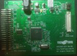
here are two photos of the board... top and bottom...

top.jpgbottom.jpg
 

Dear cyberrat
Hi
Can you explain that what is the length matching , please ?
Regards
Goldsmith

Go to transmission line theory for the answer. At high frequencies, signals change faster than they can propagate from the source to the receiver. This means there is a finite amount of time that it takes the signal to travel some distance. Since you know there is a time and a distance, you can determine a signal propagation velocity. Another way to define this phenomenon is propagation delay.

Assume you have 32 bits of data on a parallel bus (32 wires running together). If one trace is a little longer than the others, that bit may not arrive at the same time as the rest of the data, causing errors at the receiver device. To compensate for the difference in lengths, designers will add meander lines (the squiggles) to make the shorter lines physically longer. You can see that by looking at the first image. The outer-most traces are straight (longest distances to travel), while in inner ones are shorter, but have meanders added to make them closer to the same overall length as the outer-most traces.

If you've even seen a running event on a track, you may recall seeing the runners line up in staggered positions around the starting line. This is because the runner in the outside lane has a longer distance to run around the track than the person on the inside lane. By staggering them, the runners will all run the same distance to keep the race fair. This is the basic concept, just inverse of what happens on a PCB (designers make the "track" longer, by making the shorter traces zig-zag back and forth).

Meanders can induce a little bit of inductance, but not very much.... a planar spiral is a MUCH better way to add inductance using printed metal alone.
 
  • Like
Reactions: yikes

    yikes

    Points: 2
    Helpful Answer Positive Rating
shaiko on this link what you provide, this is inductors 100% or should I say school example of inductors on PCB
http://www.google.co.il/imgres?q=sp...1t:429,r:8,s:39&tx=129&ty=66&biw=1280&bih=682


I think you are wrong, I'm sure that this is inductors. You show clasicc example of inductors on PCB.


Inferring high inductance traces is something that's strongly discouraged in digital PCB design - it generates power integrity problems. Esspecialy with high switching rates.

I think that you are wrong again.


The purpose of the routing scheme at the picture is to match the length of traces and make the signals travel the same time from Tx to Rx - period.

Shaiko with full respect to You I think you are wrong again.


Here is manufacturer info about product (user guide, schematics, and previous version of PCB 2B without inductors):
Soon I will get answer from manufacturer.

http://www.techtoys.com.hk/Displays/SSD1963EvalRev3B/SSD1963 Eval Board Rev3B.htm
 

Attachments

  • Schematic.pdf
    40.1 KB · Views: 140
  • SSD1963 Eval Rev2A.pdf
    2.3 MB · Views: 154
  • SSD1963 Eval Rev3B.pdf
    1.8 MB · Views: 404
Last edited:

This is an evaluation board from Techtoys. It is a display controller board with a Solomon systech SSD1963 chip.
I am programming it with a 7" TFT display and a PIC32 from microchip. The highest frequency in that bus is the pixel clock signal that is about 12Mhz.

Yikes one correction 12MHz is multiplied with x10 and we have highest freqeuncy of 120MHz.
 

tpetar, you can trust edaboard members who are professionally equipped with high speed PCB design in this topic.

Serpentine trace patterns like the shown ones are added for length respectively signal delay matching puposes. They are primarly used in impedance matched connections, in other words the trace should be analyzed as a transmission line where the trace inductance is balanced with the capacitance.

Of course, the same shape can serve as lumped inductance under different conditions.

The present serpentine trace example shows a rough style, and I'm not sure if it's actually necessary for a pixel rate as low as 120 MHz. But the photo shows a least a broad idea of length matching.
 
  • Like
Reactions: tpetar

    tpetar

    Points: 2
    Helpful Answer Positive Rating
Status
Not open for further replies.

Part and Inventory Search

Welcome to EDABoard.com

Sponsor

Back
Top