Continue to Site

Welcome to EDAboard.com

Welcome to our site! EDAboard.com is an international Electronics Discussion Forum focused on EDA software, circuits, schematics, books, theory, papers, asic, pld, 8051, DSP, Network, RF, Analog Design, PCB, Service Manuals... and a whole lot more! To participate you need to register. Registration is free. Click here to register now.

Considering PCB trace as a transmission line

newbie_hs

Full Member level 1
Joined
Mar 4, 2023
Messages
96
Helped
1
Reputation
2
Reaction score
1
Trophy points
8
Activity points
770
Dear Team,

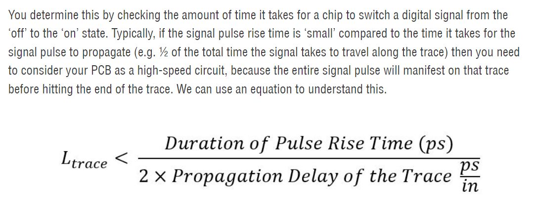
According to this link,we can consider a PCB trace as transmission line when,
1702969402972.png

I have see this explanation many places.But no one explains how transmission line effects comes when rise time is smaller than 2*times propagation delay
and how transmission line effect disappears when 2*times propagation delay is less than rise time.
Can someone please explain this.
 
t domain
Mismatched lines cause visible ringing if there is sufficient energy in 1 cycle or 2*Tpd.
To avoid this we say if rise time is greater that the period of one ring cycle, we say this is the borderline for acceptable ringing content being 1f octave down or -6dB for 1st order slope. This translates into some overshoot and ringing but tolerable. Can you compute how much?

f domain
Although exponential time constant T=RC is based on 1-1/e~ 0 to 63%, however for logic we use 10% to 90% risetime or 80% swing. Thus %T is longer by 80/63.
Meanwhile it has been proven the correlation between BW (-3dB) and rise time (10~90) is BW=0.35/Tr. If I adjust that by 80/63 , BW=0.47/Tau.
I can do an exponential filter to illustrate this with a transmission line. Delay = 100 ps 200 ohm and use characteristics for a 74ALVxx series CMOS driving with 20 ohm source =Vol/Io into a 3cm 200 ohm trace with loads equal to 10 pF.

Below the output has a resonance at 5 GHz and half power BW at 225 MHz which results in excess ringing and over/undervoltage with a 200 ohm line.
Below that without the Cap has resonance at 2.5 GHz.
1702990314951.png


Time Domain

Now showing a 100 MHz clock with a 200 ohm then a 50 Ohm line with V & I plots shown into the load cap (CMOS Input capacitance for a few gates) after 3cm line

1702991170694.png

20 Ohm T-lines would be too wide a trace for typical substrate thickness for high density logic, so 50 Ohm is adequate. But for improvement one could add 25 to 30 ohms in series with the driver and eliminate the overshoot. The ringing was near 400 MHz in the case with 200 Ohm trace.

Slightly improved result adding 10 Ohms with 2.7V PP from a 3.3V square wave

1702991901476.png


Bottom line
If you operate at the edge of this rule, you want to optimize your driver to minimize overshoot and ringing then you need to also consider trying to lower your impedance of the trace based on w/h ratio of copper trace to ground. and consider raising your source Vol/Iol best case RdsOn to match closer to the T-line impedance.

The advanced student will see I avoided trying to put 2.5GHz triangular logic into the 100 ps line. In this case, you cannot tolerate 10 pF loads and mismatched T lines. Here you might use Current Mode Logic or ECL and terminated T lines to achieve the limits of the logic technology.

p.s. Engineers even in America should not use inches for physics. ;)

Also when considering spectrum> 900 MHz, you might want to use Getek lower loss FR4 for PCB substrate and get TDR electrical testing done to confirm your T-line impedances due to 10% tolerances.
 
Last edited:

LaTeX Commands Quick-Menu:

Part and Inventory Search

Welcome to EDABoard.com

Sponsor

Back
Top