Continue to Site

Welcome to EDAboard.com

Welcome to our site! EDAboard.com is an international Electronics Discussion Forum focused on EDA software, circuits, schematics, books, theory, papers, asic, pld, 8051, DSP, Network, RF, Analog Design, PCB, Service Manuals... and a whole lot more! To participate you need to register. Registration is free. Click here to register now.

Design of Low Drop-out Voltage Regulator

Status
Not open for further replies.
Hi tompham,

I think you have implemented PKT MOK's paper. And I hope the Ccf is basically used for damping the Q. And yes, this greatly reduces the Q of the loop but inturn makes the loop ultimately slow, which will not help in Capless LDO design. I did one LDO some years back, so I would suggest you to go for a faster compensating loop, which will solve this issue. You can also try to use milliken method of making it faster, with some modifications.
 

Hi yuvan

Thanks for your suggestion. My design problem is under shoot and over shoot of output, but if zoom in the recover time for output ~2us. I think is it not slow compare to others capless LDO design. Since my Iq ~5uA (quiescent current) too small and it may cause the problem. Do you think making Iq higher will improve it? Thanks
 

Hi tompham,

May b e you can try that too. For capless LDO basically you would have made the PT gate (or the 1st stage o/p) as the dominant one, but for transient you will need the gate to react faster. So, you can make the Class AB (kind of) stage agressive which controls the gate to be much faster. And if I see it properly then you are having about 7pF as Ccf, which inherently will make it slower --> class AB operation is minimized. So, you can try reducing the damping capacitor and make it stable by introducing some other faster loop.
 

Hi tompham & yuvan,

I understand that the discussions are helpful .... but since the main post if from subbu2 so we must reply to his queries in the thread and not add our own queries ....
It will just keep this thread continuous .... Please create a separate post for your discussions .... :)
 

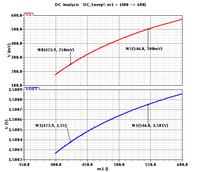
Here r d some results which i got..did the vg sweep for different values of multiplier got the results as in attachments...(W=50u L=180n)

for the power mos to be in saturation (1.62-Vg)-Vth<120mV which means Vg>0.985V (threshold was 0.515V)
also (1.62-Vg)>Vth implies Vg<1.105V... so 0.985<Vg<1.105V is the range of Vg which shud b maintained..simulation suggest dat when i keep the multilplier from abt 300 to 500 this range is satisfied..pow mos is in sat..and Vo is around 1.5015V..is this right?

So now I vary Multipliers from 400-600 i.e. W=2000u-3000u .... This time the VG node is above zero .... Now I have two option .... If need a two stage amplifier then I have to worry about only one NMOS at the output arm ... But if I need a folded cascode then I have two NMOS in the output arm .... So in the previous case around 250mV of VG will give VDS of 250mV to the NMOS and it should be sufficient .... and for the later case 500mV of VG should be sufficient for two NMOS .... I have shown two sizings that I can select ....


So if I need a two stage amplifier then my W/L = 5u*425 / 0.25u = 2125u / 0.25u
and if I need a folded cascode stage the W/L = 5u * 550 / 0.25u = 2750u / 0.25u
After the sizes are fixed check the value of VG when load current is 0mA .....

Again I have used only 1000 gain .... and see the accuracy ... 1.5003 to 1.5007 not even 1% ....

Hope this will help ... :)

I am not able to understand with Vg as low as 250mV or 500mV how can the pow mos be in saturation.?

- - - Updated - - -

new1.pngnew2.pngnew3.png
 

Yes if you can keep it in saturation then its good ... but when your Vg is 1V at 50mA then what is your Vg at 0mA load ??? Is that Vg sufficient to keep the PMOS On and as the Vg is also the drain node of the MOSFET in the output arm of the amplifier, so with 0mA load is Vg sufficient to keep the output pmos of the amplifier in saturation ???

If you are getting sufficient Vg at 0mA load for keeping the Power MOS ON & to keep the output arm mosfet of your amplifier in saturation then its great ..... else you can keep your Power MOS in linear .... In this case it will not give much gain agreed but the you can extract more gain from the amplifier .... what matters is the total gain in the loop ...
 
  • Like
Reactions: subbu2

    subbu2

    Points: 2
    Helpful Answer Positive Rating
Sir, as you mentioned if I keep the multiplier so that the power MOS is in saturation the Vg node is more than 1.4V if load is 0mA...And I found that, at 50mA load, for m=28 Vg is about 250mV and for m=37 Vg is about 500mV.. but at load current of 0mA it is increasing upto 1.35 making pow MOS to be in cutoff..

And to avoid cutoff I tried decreasing the resistances and at low resistances of 100ohms and 200ohms Vg is getting lowered eventually making pow MOS to enter saturation, at Il=0mA...but this will make more power dissipation in resistors (7.5mW) as they draw more current..

Sir, can the LDO work fine if the power MOS is in cutoff (as it is able to provide 0-50mA of load current maintaining 1.5V with minimal error)..or should i get rid of cutoff by some other way?

1.1.png1.3.png
 

Hi subbu2
I think you can make power PMOS at edge of cutoff and linear when no load and light load but make sure your LDO has high gain and good phase margin. At no load and light load the current of power PMOS small ---> Rout high ----> total gain of LDO is high. When you run ac gain you can see gain of LDO at no load and light load is higher than heavy load
 
  • Like
Reactions: subbu2

    subbu2

    Points: 2
    Helpful Answer Positive Rating
Hi subbu,

Ya it can work fine even if the Power FET is in cut-off. As the load is 0mA so there is no need for the power FET to remain ON. The voltage at the output will be held constant by the large capacitor. It will discharge through the resistor divider only. If this discharge causes the output to drop then the loop will respond and turn the Power FET ON momentarily to charge the capacitor back and again move in to cutoff.

But turning the PFET ON from cut-off will make the loop slow so load regulation results will be degraded. But as long as it is with in spec or tolerable it should be fine ..
 
  • Like
Reactions: subbu2

    subbu2

    Points: 2
    Helpful Answer Positive Rating
Thank you sir.

I will now proceed for the design of folded cascode diff amp. Sir what are the parameters to aim at and what is the gain that I can expect from the topology.?
 

  • Like
Reactions: subbu2

    subbu2

    Points: 2
    Helpful Answer Positive Rating
Thank you sir.

I will now proceed for the design of folded cascode diff amp. Sir what are the parameters to aim at and what is the gain that I can expect from the topology.?

hi..

the important thing in cascode design is it should be in saturation over the operating voltage range..

so try to size the devices accordingly..

and the output impedence of this design should be high which is needed for a greater gain,,
 
  • Like
Reactions: subbu2

    subbu2

    Points: 2
    Helpful Answer Positive Rating
Thank you sir.

I will now proceed for the design of folded cascode diff amp. Sir what are the parameters to aim at and what is the gain that I can expect from the topology.?

Hi subbu,

Looking back to your first post in this thread .... your LDO output accuracy was +/-3% and the reference itself varies +/-1% ... So you are left with +/-2% accuracy ...
Now there will be gain error and offset due to mismatch in the error amplifier ... all of this should be within +/-2% ....

Now 2% of 1.5V (Output of LDO) is 30mV .... So you have to split up between gain error and mismatch offset ....
1) Targeting a loop gain of above 60dB (1000) should give you less than 1mV variation
2) Target not more than 10mV offset from the error amplifier

So you are left with 30mV - 11mV = 19mV of variation ..... which will be consumed by load and line regulation ...
So before starting with the amplifier design, just try to find out how much gain is being contributed by the Power FET (i.e. gain from Power FET gate to LDO output) both in 50mA load and 0mA load (Note: gain will widely vary with load change) keeping the lowest achieved gain in to consideration ... say XdB gain .... try to find a suitable architecture for the error amplifier that will give you Gian > 60dB - X ....

Hope this will help ... :)
 
Status
Not open for further replies.

Part and Inventory Search

Welcome to EDABoard.com

Sponsor

Back
Top