Continue to Site

Welcome to EDAboard.com

Welcome to our site! EDAboard.com is an international Electronics Discussion Forum focused on EDA software, circuits, schematics, books, theory, papers, asic, pld, 8051, DSP, Network, RF, Analog Design, PCB, Service Manuals... and a whole lot more! To participate you need to register. Registration is free. Click here to register now.

Problem about how to choose the voltage level of output device when designing a moto driver

newbie2023

Newbie level 4
Joined
Dec 7, 2023
Messages
6
Helped
0
Reputation
0
Reaction score
0
Trophy points
1
Activity points
46
Hi everyone,
I'm studying design a moto driver circuit. I feel confused about how to choose the devices.
If the bus voltage = 40V, and the Vbs = 15V. Is the 16V nldmos/pldmos(BV=18V@MIN,25@TYP)enough for my design?
Or I should choose 60V devices which is greater than 40V + 15V ?
Thanks a lot!
 
It depends on the driver topology. In usual full bridge topology, transistors must be rated for bus voltage plus margin for overvoltage generated at parasitic circuit inductance by current di/dt. 60V rating sounds like a reasonable choice for 40V bus and carefully designed PCB.
 
It depends on the driver topology. In usual full bridge topology, transistors must be rated for bus voltage plus margin for overvoltage generated at parasitic circuit inductance by current di/dt. 60V rating sounds like a reasonable choice for 40V bus and carefully designed PCB.
Thanks for ur reply. It is a H-bridge topology indeed.
motojpg.jpg

Because the voltage between Drain and Source is VBS. When HO is low, the Max voltage among Drain and Source of high-side driver is VBS. 60 V device cost too much layout area😭 . I'm not sure whether choose 1.5*VBUS or 1.5*VBS.
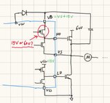
 
The question isn't quite clear. Are you asking about gate driver or H-bridge power transistors?

H-bridge has to be rated for Vbus + margin, gate driver for Vbs +.
 
  • Low RdsOn FETs in 2x half or 1x full bridge are needed with high side for direction control and low side for PWM acceleration ramp and speed with charge pump cap and diode for Vboot(VB) to rise above V+ for Pch gate drive.
  • Determine Motor coil resistance (DCR) and choose RdsOn ~5% of DCR give or take as lower Rdson also raises Coss and series LCR Q resonance and higher Ron increases losses.. Clamp diodes for output are needed and on V+ with low side PWM on-off which must handle same current as FETs also have capacitance that increases with power rating. Fast Recovery types cost more but reduce C.
  • Use loose twisted pairs to motor to reduce emissions.
  • Simulate losses and double the heat sink requirements to have better thermal rise.
  • Estimate max acceleration, brake, stop, reverse specs to minimize peak power demands with inertia for control system, which can be 10x max rated load power in one direction and 20x in full reverse.
  • Limit current by sensing it in servo loop.
  • Add RPM sense if you want speed control.
 
I would suggest overdesigning the power path, what's the
real difference in cost between a "60V" FET and a "100V"
FET? Start dead reliable and then swap in cheaper on
some board builds to see where failure rolls on? Maybe
better than starting weak and doing repetitive debug
of smoked boards.

Do you have any crazy problems like the motor is in a
traction application with a gearbox, and a downshift
when RPM is near max could overspeed the motor and
back-EMF your driver into toast?
 
Also realize that while Rdson induces switching losses, but too low and you have a high Q resonant RLC circuit. Remember this.

High Q relies on snubber diodes to dissipate heat or a brake resistor if there is a lot of inertia.

Also when commutating both FETs in a half-bridge , ensure you have near 1us of dead time to avoid shoot-thru failures. this method is used to maintain high torque with speed control and at least one drive hi or low active. But don't worry about that for now. A ha;lf-bridge needs a bipolar supply for bi-directional control, but it's usually less expensive to use a single supply and full bridge.
 
The question isn't quite clear. Are you asking about gate driver or H-bridge power transistors?

H-bridge has to be rated for Vbus + margin, gate driver for Vbs +.
I'm sorry if my expression caused any confusion. I am studying the design of an H-bridge structure gate driver chip for driving a motor. The bus voltage is 40V. The current focus is on the output stage of the driver chip.
motojpg.jpg

According to your reply, I should choose based on the VBS voltage. How much margin is approximately needed? For a 15V VBS voltage, is it sufficient to choose 15V nLDMOS/pLDMOS (BV=18V@MIN). Or should I opt for devices with a higher voltage rating? Currently, the available PDK I have supports only 5V/15V/60V.
Thank you again for your reply.
 

Attachments

  • motojpg.jpg
    motojpg.jpg
    252.3 KB · Views: 52
Last edited:
  • Low RdsOn FETs in 2x half or 1x full bridge are needed with high side for direction control and low side for PWM acceleration ramp and speed with charge pump cap and diode for Vboot(VB) to rise above V+ for Pch gate drive.
  • Determine Motor coil resistance (DCR) and choose RdsOn ~5% of DCR give or take as lower Rdson also raises Coss and series LCR Q resonance and higher Ron increases losses.. Clamp diodes for output are needed and on V+ with low side PWM on-off which must handle same current as FETs also have capacitance that increases with power rating. Fast Recovery types cost more but reduce C.
  • Use loose twisted pairs to motor to reduce emissions.
  • Simulate losses and double the heat sink requirements to have better thermal rise.
  • Estimate max acceleration, brake, stop, reverse specs to minimize peak power demands with inertia for control system, which can be 10x max rated load power in one direction and 20x in full reverse.
  • Limit current by sensing it in servo loop.
  • Add RPM sense if you want speed control.
Thank you for your reply! It has taught me a lot. I've recently started learning about gate driver technology. Regarding the engineering experiences you mentioned in your reply, are there any books or papers that you can recommend or provide keywords for? Thank you again!(y)
 
I would suggest overdesigning the power path, what's the
real difference in cost between a "60V" FET and a "100V"
FET? Start dead reliable and then swap in cheaper on
some board builds to see where failure rolls on? Maybe
better than starting weak and doing repetitive debug
of smoked boards.

Do you have any crazy problems like the motor is in a
traction application with a gearbox, and a downshift
when RPM is near max could overspeed the motor and
back-EMF your driver into toast?
Overdesign initially, then gradually optimize the design to reduce costs. The perspective you provided is very valuable. Thank you very much!(y)
 
O.k., maximum voltage difference on low+high side driver chip is obviously Vbus + Vbs + possible overshoot. Confusingly you have been asking for HS driver transistor rating only. But there will be also a level shifter and isolation between high side island and substrate.
 
O.k., maximum voltage difference on low+high side driver chip is obviously Vbus + Vbs + possible overshoot. Confusingly you have been asking for HS driver transistor rating only. But there will be also a level shifter and isolation between high side island and substrate.
Thank you for your reply! It is not a floating island process which the floating island tolerates high voltage. In this process each device has its own independent isolation structure. I don’t know if I made myself clear. Do you mean I should add a HV ring to surround the high-side devices?
 
A ring won't save you. You need either triple well or SOI
if you mean to swing the high side source to VIN using
NMOS. Of course you can, and I have, used PMOS high
side. But then the NWell has to be high voltage (triple
well gives you the HV NWell in which PWell or NWell can
sit, protected). You will have rings and you will need to
take extra care about breaking up devices to keep the
isolation junction, which is the base of a parasitic HV PNP,
from turning on the emitter-base (DNW - PWell or
DNWell-P+). "Common Mode Transient Immunity" presents
a problem for faster FETs & GaN, the jerk can break your driver.

I much prefer SOI but the P/L guy will whine about the extra
starting-material cost. You could discuss the pros & cons to
look like a guy who knows his process options, if it's that kind
of a party.
 

LaTeX Commands Quick-Menu:

Part and Inventory Search

Welcome to EDABoard.com

Sponsor

Back
Top