Continue to Site

Welcome to EDAboard.com

Welcome to our site! EDAboard.com is an international Electronics Discussion Forum focused on EDA software, circuits, schematics, books, theory, papers, asic, pld, 8051, DSP, Network, RF, Analog Design, PCB, Service Manuals... and a whole lot more! To participate you need to register. Registration is free. Click here to register now.

Self-Oscillation in Wideband High Gain Ultra Low Noise Amplifier

Alipoursaadaty

Member level 3
Joined
Dec 4, 2015
Messages
60
Helped
0
Reputation
0
Reaction score
0
Trophy points
1,286
Activity points
13,629
Hello,

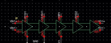
I am an IC designer and have designed open-loop amplifiers with about 80 dB voltage gain and 200 MHz bandwidth. The structure of the amplifiers is a 4-stage 20 dB amplifier with a buffer at the output (it is a 5-stage with a buffer). As I designed this amplifier in open-loop mode, I expected to prevent instability and oscillation. However, I am now measuring the fabricated chip in 65 nm TSMC tech. Would you please let me know if the grounding and VDD loops cause this oscillation? I connected all the grounds of each stage in the layout. However, the VDD of the first stage and buffer are unique and are separated from the second, third, and fourth stages. The voltage bias of the transistors is generated by the bias method and common-mode feedback circuits. Self-bias loop gains are so small and cannot create oscillation.

In the measuring, I can tune the voltage bias of some transistors to control the gain. By reducing the voltage gain to 40, 50, and in some cases 60 dB, oscillation is going to be suppressed. Also, the oscillation frequencies are almost higher than 100 MHz to 2 GHz. However, most of them are near the 1 GHz.

During the post-layout simulation, there was no oscillation in these amplifiers. How can I model this oscillation in the Cadence? In other words, why was not the oscillation seen in the post-layout simulations?

Is there anyone to help me to find out the main problem?

Regards,
 

Attachments

  • 5-Stage Amplifier.jpg
    5-Stage Amplifier.jpg
    28.3 KB · Views: 51
Usually you pay special attention to filtering the power supply as you move from the output to the input, if not you can get issues, when filtering this way the semis working with the smallest signals have the cleanest power supply, and inversely so as you more to the higher power output,

failure to do this can result in psu induced oscillation, the the psu conducts signals, or is modulated by the power stages back to the input stages and affects them.
Thank you for your response.

I separated the psu of the first stage VDD from the others with 1V. Also, the last stage is buffer working with 2.5V psu. I soldered 100pF, 10nF, 220nF, and 1uF decoupling caps to filter the noises. Also, Inside of the layout I put decoupling caps for power supply nodes of about 20pF which is a little bit small. However, the VDD of stages 2, 3, and 4 are connected before the caps.

Moreover, my architecture for each stage is a fully differential amplifier (FDA). Also, the total structure is FDA. However, by doing this, the oscillation problem was not solved.

On the other hand, the ground nodes are connected inside of the layout from stages 1 to 5. One scenario can be this. However, as the structure is fully differential, there must be a virtual ground in AC mode in the circuit.

I should mention that the maximum CMRR is 60 dB. Thus, the common mode signal (noise) can be amplified with at least 20 dB. Also, the earth and ground of our lab have some noises at 20 MHz and 95 MHz. However, these are not the oscillation frequencies.
 
Start with modeling the bond wire, package, socket and close-in
board parasitics and passives (and the internal nonidealities of
those). Or probes. Whatever.

Weak decoupling and an inductive supply feed with an amplifier
across it, sitting on a mesh of R, L, C and mutuals, what could go
wrong?
 
80 dB Voltage Gain is too much for an Integrated Amplifier chain.
Is it a compulsory specification or something else ? It seems to me too much. It's so difficult to maintain the stability over this amplifier chain.
A small feedback with near to zero phase shift will make it to oscillate. And unfortunately this might not be visible during even extracted view simulation.
Bonding scheme, GND connections, VDD connections etc. play very strong role on the overall stability. The amplifier might oscillate even off-chip.
 
Start with modeling the bond wire, package, socket and close-in
board parasitics and passives (and the internal nonidealities of
those). Or probes. Whatever.

Weak decoupling and an inductive supply feed with an amplifier
across it, sitting on a mesh of R, L, C and mutuals, what could go
wrong?
Thank you for your attention. According to the bond wire effect, I simulated its effect before fabrication. Also, I remove the package and socket and directly wire bond to the PCB. However, the bond wires are so long in this situation (about 1 cm for each one).

Due to weak decoupling and an inductive supply, I checked the power supply by the signal analyzer, and the oscillation frequency can be found on the spectrum. When I check the power supply node by a probe from the signal analyzer, the weakened noise can be seen there. However, I put some ceramic caps mentioned above in the size of 0402. Also, I attempt to put large capacitors, but the oscillation is not removed. As I put voltage tuning to control the gain of the amplifier, when I reduce the gain to 40 dB or 50 dB, the oscillation is removed and the amplifier amplifies the input sine wave by this voltage gain.
--- Updated ---

80 dB Voltage Gain is too much for an Integrated Amplifier chain.
Is it a compulsory specification or something else ? It seems to me too much. It's so difficult to maintain the stability over this amplifier chain.
A small feedback with near to zero phase shift will make it to oscillate. And unfortunately this might not be visible during even extracted view simulation.
Bonding scheme, GND connections, VDD connections etc. play very strong role on the overall stability. The amplifier might oscillate even off-chip.
Thank you for your response.

These specifications are necessary to achieve. I put resistive feedback to self-biasing the input transistors at the first stage, and common mode feedback for other stages. Also, there are some AC coupling capacitors between stages 2-3 and 4-5 to separate their DC bias from each other. Therefore, there is resistive feedback in stages 3 and 5. However, there is no total feedback between the input and output nodes of the amplifier. Although there are some loops between VDD and ground connections, there are some virtual grounds in every stage to prevent every noise coming from VDD and GND as it is a fully differential architecture.

About the bonding scheme, I tried to wire bond input and output pins from different paths. and keep the distance between VDD wires. Also, the VDD of the first stage has been separated from other stages' VDDs, but the VDD of stages 2, 3, and 4 are connected and also, the VDD of stage 5 has been separated. However, in the spectrum of the VDD in the first stage, the frequency oscillation of the amplifier can be seen (so strange). Would you please inform me if you know the reason for this happening? Also, how can I model this oscillation after layout extraction?
 
Last edited:
A well as your caps to gnd you need series impedance between stages to effect real filtering, usually, 4E7, 10E, 22E, 47E and so on as you proceed to the stages with the smallest input signals.
 
Thank you for your attention. According to the bond wire effect, I simulated its effect before fabrication. Also, I remove the package and socket and directly wire bond to the PCB. However, the bond wires are so long in this situation (about 1 cm for each one).

Due to weak decoupling and an inductive supply, I checked the power supply by the signal analyzer, and the oscillation frequency can be found on the spectrum. When I check the power supply node by a probe from the signal analyzer, the weakened noise can be seen there. However, I put some ceramic caps mentioned above in the size of 0402. Also, I attempt to put large capacitors, but the oscillation is not removed. As I put voltage tuning to control the gain of the amplifier, when I reduce the gain to 40 dB or 50 dB, the oscillation is removed and the amplifier amplifies the input sine wave by this voltage gain.
--- Updated ---


Thank you for your response.

These specifications are necessary to achieve. I put resistive feedback to self-biasing the input transistors at the first stage, and common mode feedback for other stages. Also, there are some AC coupling capacitors between stages 2-3 and 4-5 to separate their DC bias from each other. Therefore, there is resistive feedback in stages 3 and 5. However, there is no total feedback between the input and output nodes of the amplifier. Although there are some loops between VDD and ground connections, there are some virtual grounds in every stage to prevent every noise coming from VDD and GND as it is a fully differential architecture.

About the bonding scheme, I tried to wire bond input and output pins from different paths. and keep the distance between VDD wires. Also, the VDD of the first stage has been separated from other stages' VDDs, but the VDD of stages 2, 3, and 4 are connected and also, the VDD of stage 5 has been separated. However, in the spectrum of the VDD in the first stage, the frequency oscillation of the amplifier can be seen (so strange). Would you please inform me if you know the reason for this happening? Also, how can I model this oscillation after layout extraction?
Since we don't know about all those stuff (bonding, grounding, VDD distribution, packaging, etc.) it's hard to say something. If you see that oscillation on VDD off-chip line, decoupling is also problematic. There might be other internal-external issues that fail this amplifier.
 
80 dB Voltage Gain is too much for an Integrated Amplifier chain.
There are many Op Amps with >= 100 dB DC gain and GBW > 1GHz, however they tend to be well compensated for adequate phase margin or minimal peaking at some minimal load capacitance. They tend to have low DC output impedance. The recommended layouts tend to guard the I/O's with adequate ground fill and minimal parasitic ESL to the test port. There are not many OA's with more than 12 GHz GBW. These general purpose (GP) types tend to have GBW/-3dB BW < 10.

Without know your design specs for purpose and layout, it is impossible to say much more. Is it a GP type or special purpose.

e.g. https://www.ti.com/lit/ds/symlink/opa892.pdf 100dB = Aol, NPN type.
 
I simulated 1cm wirebonds are about 5to8 nH +/-? % with say 5pF load
Does this resonate near yours?
Then any positive feedback parasitic coupling to high Z inputs will make a fine osc.
View attachment 188225View attachment 188226
That is a good point. As I wire bonded to PCB with long wire bonds, it is probable to oscillate due to this reason. Also, one of the main oscillation frequencies is this one. I changed the output wire bond lengths for one die by about 30% and could measure it. The gain was 60 dB, and the 3-dB bandwidth is higher than 240 MHz (I did not have a high-frequency waveform generator greater than 240 MHz). However, there was a strange thing. The input referred noise in measurements was half of the schematic simulation. Also, there are some other frequencies in the spectrum in the frequencies of 1 GHz, 800 MHz, 700 MHz, ....


IMG_5211.jpg


Maybe because of these noises, the voltage gain is reduced by 18 dB compared to the simulation results. Also, the output nodes' DC bias are different from each other (475 and 520 mV). These measurements have been done without an output buffer stage.

How can I model this wire bond effect for differential input and output nodes? Also, do you determine the oscillation frequency by resonant formula? (1/sqrt(L*C))

Before the fabrication, I modeled the wire bond effect. However, I thought the cap would be less than 500 fF.

Moreover, the cables used in the measurements have 32 pF/ft (100 pF/m) capacitance. Should I model them in my simulation or not?

About high-Z input, my designed amplifier does not have high-Z input, and it is less than 500-Ohm.
--- Updated ---

A well as your caps to gnd you need series impedance between stages to effect real filtering, usually, 4E7, 10E, 22E, 47E and so on as you proceed to the stages with the smallest input signals.
Sorry, I didn't realize how I should connect the impedances and which caps must be placed.
--- Updated ---

There are many Op Amps with >= 100 dB DC gain and GBW > 1GHz, however they tend to be well compensated for adequate phase margin or minimal peaking at some minimal load capacitance. They tend to have low DC output impedance. The recommended layouts tend to guard the I/O's with adequate ground fill and minimal parasitic ESL to the test port. There are not many OA's with more than 12 GHz GBW. These general purpose (GP) types tend to have GBW/-3dB BW < 10.

Without know your design specs for purpose and layout, it is impossible to say much more. Is it a GP type or special purpose.

e.g. https://www.ti.com/lit/ds/symlink/opa892.pdf 100dB = Aol, NPN type.
Thank you for your attention on this matter.

It has a special purpose. The specification is like this:

Voltage gain > 70 dB
BW > 500 MHz
Ni < 3 (nv/sqrt(Hz))

However, the gain and BW can be converted. For example, the gain can be 76 dB and BW 250 MHz.

Therefore, the compensation can't be done for this amplifier due to a reduction in performance for less than the specs.

The recommended layouts tend to guard the I/O's with adequate ground fill and minimal parasitic ESL to the test port.
Also, according to this comment, I connected the input and output nodes to simple pads like the GNDs and VDDs in the layout. Should I use any specific method to connect them like using guard rings around the input and output pads?
 
Last edited:
That is a good point. As I wire bonded to PCB with long wire bonds, it is probable to oscillate due to this reason. Also, one of the main oscillation frequencies is this one. I changed the output wire bond lengths for one die by about 30% and could measure it. The gain was 60 dB, and the 3-dB bandwidth is higher than 240 MHz (I did not have a high-frequency waveform generator greater than 240 MHz). However, there was a strange thing. The input referred noise in measurements was half of the schematic simulation. Also, there are some other frequencies in the spectrum in the frequencies of 1 GHz, 800 MHz, 700 MHz, ....


View attachment 188242


Maybe because of these noises, the voltage gain is reduced by 18 dB compared to the simulation results. Also, the output nodes' DC bias are different from each other (475 and 520 mV). These measurements have been done without an output buffer stage.

How can I model this wire bond effect for differential input and output nodes? Also, do you determine the oscillation frequency by resonant formula? (1/sqrt(L*C))
Find a tool that computes L from length/width ratio and height above ground. L increases by log of l/w or l/r ratio so very thin wires can be > 1 nH/mm.
Differential wires reduce L by mutual coupling but add if wide apart as a self-inductance.
1706560485025.png

1706559240895.png

Before the fabrication, I modeled the wire bond effect. However, I thought the cap would be less than 500 fF.
Moreover, the cables used in the measurements have 32 pF/ft (100 pF/m) capacitance. Should I model them in my simulation or not?
About high-Z input, my designed amplifier does not have high-Z input, and it is less than 500-Ohm.
Sorry, I didn't realize how I should connect the impedances and which caps must be placed.
Thank you for your attention on this matter.
You should model everything that matters including skin effects and parasitic fF coupling. Use a pen sized rare-earth magnet to find areas of ESL sensitivity and poke with finger or hand near board/chip to find areas of crosstalk sensitivity to observe effects where a circuit may benefit from a foil shielding can. We always used cans over hybrid LNA's/Rx/VCO's for 1GHz and I made them for prototypes from a local PCB shop using brass foil with 50% etching on one side for fold lines and both sides for cuts. Then Zinc plated in a tank from etched foils to make them solderable and get them made in a day or 2 with gerber files and a PO sent by FTP. This yielded very high quality results like production custom EMI shields. Anything that affects spurious signals can be diagnosed easier this way then suppressed by design mitigation.
It has a special purpose. The specification is like this:
Voltage gain > 70 dB
BW > 500 MHz
Ni < 3 (nv/sqrt(Hz))

However, the gain and BW can be converted. For example, the gain can be 76 dB and BW 250 MHz.

Therefore, the compensation can't be done for this amplifier due to a reduction in performance for less than the specs.


Also, according to this comment, I connected the input and output nodes to simple pads like the GNDs and VDDs in the layout. Should I use any specific method to connect them like using guard rings around the input and output pads?
For < 5% wavelength use the lumped element values.
For lower ESL use Litz wire outside chip and match conjugate impedances with a filter where necessary. I would use an SMA near chip for semi-rigid coax for best test results.
Whenever I see users testing high speed logic (e.g. 1~2ns=Tr) with overshoot, I know they have ESL on a long ground clip of the 10:1 probe and/or too low an impedance source with a 50 Ohm load so adding 20 to 30 ohms at driver eliminates the overshoot. This is passive amplification at LC resonance.
 
See if you can make 2 stages with 40 dB gain to work then cascade them with adequate isolation or 3 inverting stages and 1 inverting stage with good isolation. But 80 dB gain non inverting is just asking for trouble, even if differential as the CM gain becomes important.
 
Last edited:

LaTeX Commands Quick-Menu:

Part and Inventory Search

Welcome to EDABoard.com

Sponsor

Back
Top