Continue to Site

Welcome to EDAboard.com

Welcome to our site! EDAboard.com is an international Electronics Discussion Forum focused on EDA software, circuits, schematics, books, theory, papers, asic, pld, 8051, DSP, Network, RF, Analog Design, PCB, Service Manuals... and a whole lot more! To participate you need to register. Registration is free. Click here to register now.

How to determine if noise/voltage spike is too high for MCU?

pgib8

Member level 2
Member level 2
Joined
Aug 9, 2016
Messages
44
Helped
1
Reputation
2
Reaction score
3
Trophy points
1,288
Activity points
1,824
Hi, I'm getting a voltage spike from a power supply and I'm measuring it directly at the microcontroller (MCU). I know that it exceeds the absolute maximum rating but it is extremely bief. You can see below that it is about 10 V and the absolute maximum rating for the MCU is 4 V, however it appears to only last for maybe 20 ns. When it comes to damage all I know is that it is the heat that causes the damage, so because of how short it is, it will not be enough energy to do this. What I don't know is if even a very short pulse like this can cause damage. Also it is not only 1 spike but there are a lot of them. Of course if it was me, I would have seen to it that this gets filtered out for good measure but the source of this is done by another person. I have to decide for myself if I tell them that this needs to be fixed or if this is completely normal and/or should be ignored. See scope shots below.

The only thing that tells me that it is OK is the following from the datasheet:
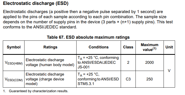
1699636710100.png


Does that mean that I can ignore these spikes? If yes, then I have to check the same for every other IC on the board that is exposed to this for the same?
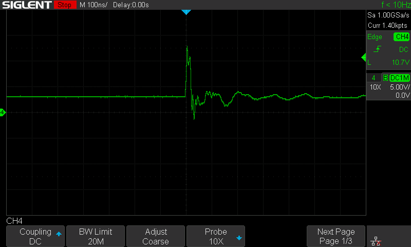
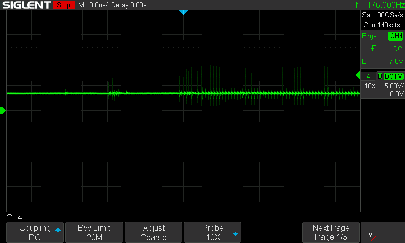
1699636083629.png


1699636332007.png
 
Hi,

"a voltage spike from a power supply" surely is way different to a low energy ESD pulse.

You definitely should check the ANSI/JEDEC standards and do some energy calculations.

BTW: Properly installed bypassing capacitors make it about impossible to get a 20ns 10V pulse at VCC.
And if it really happens then the pulse current and the according energy is way too high.

Mind: power supply is "wired" whereas "ESD" is a spark with a high series impedance.

Klaus
 
Thanks @KlausST, what you are saying makes a lot of sense. There are a ton of bypass capacitors all along the way to where I'm measuring from.
 
How did you generate this pulse? ESD generator (HBM = 100 pF) If so then there is a natural voltage divider ratio. The 20 MHz ringing on top of a flat pulse is most likely your 10:1 probe ground ringing. Current should be measured as it is likely non-linear with voltage.

Your typical LDO will have a BW of 50 kHz or > 5us. The higher frequencies must be attenuated by the ESR*C=Tau of your decoupling caps.

What causes these many spikes?
--- Updated ---

Does that mean that I can ignore these spikes? If yes, then I have to check the same for every other IC on the board that is exposed to this for the same?


View attachment 186173
Consider that a uC has both static and dynamic impedance. For the duration of this 20 ns pulse, can we assume the uC is static? only in between clock transitions. During transitions, all active Pch and Nch FETs will draw high currents.
 
Last edited:
Presuming the voltage magnitude between VCC and GND pins is actuality as shown in the waveform.
1. ESD specs don't directly apply because they are charge/current based, as stated.
2. I'd nevertheless assume that even low level ESD (e.g. 500 V contact discharge) generates higher pulse than 10 V.
3. Biggest problem is that ESD specs don't expect simultaneously applied supply voltage. With supply voltage, even small surges can cause destructive latch-up, depending on IC technology details. Only empirical tests can prove device safety.
 

Attachments

  • 8 Tips for Better Scope Probings.pdf
    1.9 MB · Views: 126
  • ABCs-of-Probes_Primer_60W-6053-16.pdf
    8.9 MB · Views: 118
  • Oscilloscope Probing for High-speed Signals.pdf
    2.2 MB · Views: 133
Last edited:
Thanks @KlausST, what you are saying makes a lot of sense. There are a ton of bypass capacitors all along the way to where I'm measuring from.
This is not acceptable to see > 10V 20 ns spikes at > 1MHz rep. rate on a 3.3V rail.
Either it is a measurement error or a serious ingress problem.
Either way, it must be fixed.

If this is coupled noise from some arc noise, then measurement errors are likely.

The appropriate test method should then be with a 50 Ohm terminated DSO using 50 ohm coax AC coupled to the DC rail.
 
You are initially asking if a 3.3V device will likely survive 10V/20ns supply surge returning to regular 3.3V. I tried to explain that this can't be guaranteed but behaviour rarely predicted from datasheet. Chip designer will most likely know.

Next question would be if device can be protected though.
 
There are non-thermal failure modes as well as simple I^2*R,
in CMOS technologies your gate ox rupture voltage is likely
2X long term, 3X short term, the rated max VDD. You're on a
3.3V I/O rail I expect. I worked on a flow of similar voltage,
that saw bare FET-quad mixers deliver 10V HBM (yes) ESD
test results. You have a sack of weak links, which one breaks
depends some on what you hit.
 
Wow, thank you all so much for this valuable information. I also thought it was not OK and there is no reason to have a power source this bad, at least not for things involving a microcontroller and other similar components.
The source of the noise is indeed from arcing on a relay. The person that designed the board where this "noise" comes from didn't do any kind of snubber on the relay contacts and for testing purposes I'm switching an inductive load, and when turning the relay off, there are many arc re-ignitions on the contacts which transfer through the power supply. My other post would have the details on that and includes the schematic: https://www.edaboard.com/threads/sw...g-waveform-on-scope-i-dont-understand.408994/

I can now say with confidence that this design will potentially be problematic and potentially severely impact the reliability of the device as a whole.
Consider there are 4 types of snubbers, R, C, RC and diode/zener depending on AC or DC and leakage current permitted. Lossy film caps are most popular for AC so that close currents are not too high. Snubbers help to restore some lost MTBF due to negligent arc switching where 10e6 mechanical ratings for contacts quickly erode to 10e3 switches with surface temperatures > 5000'K from the detonation of air.

This is why Omron, the best relay supplier in the world now promotes solid-state switches with ZVS and ZCS. This is also a good reason for you to get the design changed to a better ZCS power switch. These days even though they show an opto-coupled triac on the outside simplified schematic, inside they use milliohm FET switches with a diode bridge and an RF coupled isolated gate driver which is more reliable than opto-semis due to the 300% hFE wide variance in CTR. You still need snubbers for DC inductive switching but those are just semiconductor types.

In my last exercise reversing the direction of a 100W 120V AC 50,000 CFM fan, I was surprised to find it was not isolated and used a 3-phase FET bridge for a 3-phase 100W motor speed-controlled by an STM32 micro with a pot.

Conclusion
=======

> Either it is a measurement error or a serious ingress problem.
in this case, it was both. It happens all the time. Better to learn now in the design phase how to measure EMI with a shorted 10:1 probe for near-field radiated noise and for conducted supply noise, use AC-coupled 50 ohms coax terminated at DSO.

- trust your instincts next time and your fundamentals.
Do not accept false signal captures without explanations.
Learn how to conduct better test methods for DC noise ingress and egress. (They don't teach this stuff in school, but I can save you time.)
--- Updated ---

-Back in the early '80s when a large network we designed, we needed to know how much EMI we could tolerate error-free for the long-distance serial communication.

An oscillating relay with an inductive arc load or a brushed AC motor was a pretty good test on a long cable. But ESD in the dry winter to a keyboard was the most overlooked fault. Arcs could even go around exposed LED's to latch up the CMOS until they realized a light pipe was needed. Shannon-Hartley's Law, Arrhenius Law , Ohm's Law and Coulomb's Law were all pretty handy to know.
 
Last edited:

LaTeX Commands Quick-Menu:

Part and Inventory Search

Welcome to EDABoard.com

Sponsor

Back
Top