samiran_dam
Full Member level 2
Hi all,
I am not very knowledgeable in digital circuit. That;s why I need a bit help from you.
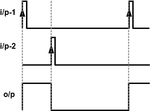
I have two i/p signals: i/p-1 and i/p-2 as shown in the following image. From the these two inputs I need to generate the output as also shown in the image.

Please note that the inputs are very narrow pulses. So, I have to rely on there positive edges. SR latch is not working as I have tried.
Please help.
- - - Updated - - -
Hi,
A NOR gate based SR latch seems to be the working solution. When I simulate the latch in LTSpice, I am getting the intended o/p. However, in Cadence Spectre simulator the simulation throws a convergence issue. Any help?
I am not very knowledgeable in digital circuit. That;s why I need a bit help from you.
I have two i/p signals: i/p-1 and i/p-2 as shown in the following image. From the these two inputs I need to generate the output as also shown in the image.

Please note that the inputs are very narrow pulses. So, I have to rely on there positive edges. SR latch is not working as I have tried.
Please help.
- - - Updated - - -
Hi,
A NOR gate based SR latch seems to be the working solution. When I simulate the latch in LTSpice, I am getting the intended o/p. However, in Cadence Spectre simulator the simulation throws a convergence issue. Any help?