- Joined
- Apr 1, 2011
- Messages
- 15,183
- Helped
- 2,900
- Reputation
- 5,812
- Reaction score
- 2,982
- Trophy points
- 1,393
- Location
- Minneapolis, Minnesota, USA
- Activity points
- 113,743
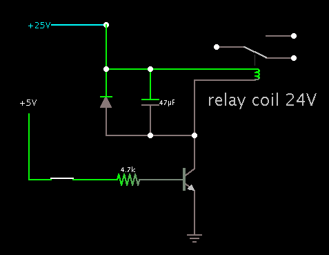
is it a circuit of charge pump relay drive circuit?
I have made a simulation of the middle section.
The capacitors do not have what is specifically called charge pump action. They are exposed to alternating current square waves.
The transistors create push-pull action. This results in current going around an upper loop and a lower loop.
AC goes through the combination of C1 - D1 - D4 - R7.
Notice the diodes both point toward X1. This creates a high positive volt level at X1.
Similarly Y1 is at a low volt level. (Notice the neighboring diodes point away from Y1.)
One is reminded how AC is converted to DC by a conventional diode-bridge power supply.
When the transistors are off, the capacitors block all DC. The right hand section receives no current. (I was wrong about the charge bleeding off when idle. The capacitors acquire a greater DC charge when idle, than they had while the action was going.)
We might wonder why a DC supply is converted to AC, and then back to DC. I believe it must be a safeguard, with the aim to disconnect the relay from all power rails.