giorgi3092
Junior Member level 2
Hi,
I am doing a layout of a NAND gate.
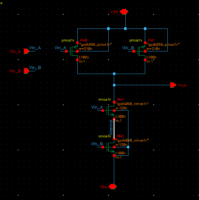
I built the following schematic:

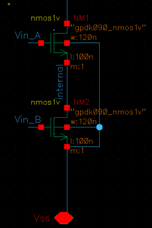
The problem is with the NMOS pull-down network so here's a close up:

From this screenshot, it is clearly visible that the upper NMOS's and lower NMOS's bodies are connected together and it is connected to Vss (i.e. gnd).
Also note that the wire "internal" is the one connecting the source of upper NMOS and drain of the lower NMOS.
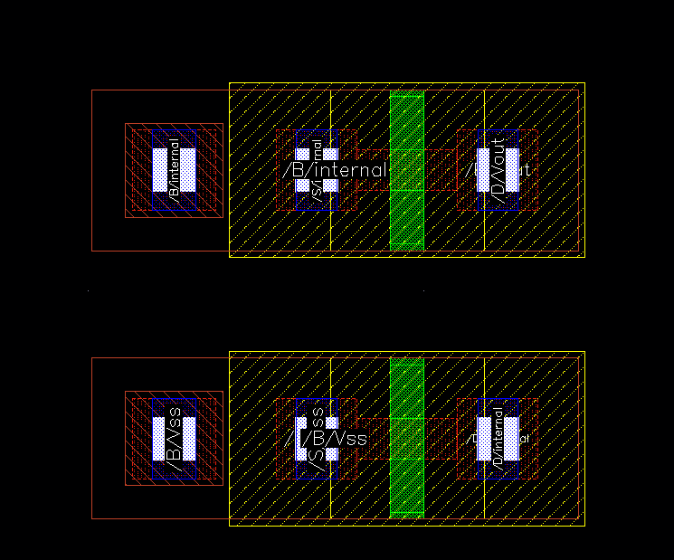
So, now let's go to the layout where I believe the mismatch occurs. I use "Generate from source" and all other default settings. Then I switch the transistor "bodytie" setting to detached to show the body clearly. Here it is:

The upper transistor is the upper NMOS and the lower transistor is the lower NMOS as in the schematic above.
Now, if we look at the upper NMOS and compare it with the schematic: in the schematic, the body is connected to Vss and source is connected to the "internal" wire. However, for some reason, in the layout as shown right here it shows that both body and source are connected to the "internal" wire. Can anyone explain what is going on?
And if I proceed with the layout like this I get DRC errors such as Psubstrate_connErrorMult, or something like this.
I expected that upper NMOS's body would show as connected to Vss instead of the "internal" wire. But, it's not the case....
What could be the problem?
Giorgi
I am doing a layout of a NAND gate.
I built the following schematic:
The problem is with the NMOS pull-down network so here's a close up:
From this screenshot, it is clearly visible that the upper NMOS's and lower NMOS's bodies are connected together and it is connected to Vss (i.e. gnd).
Also note that the wire "internal" is the one connecting the source of upper NMOS and drain of the lower NMOS.
So, now let's go to the layout where I believe the mismatch occurs. I use "Generate from source" and all other default settings. Then I switch the transistor "bodytie" setting to detached to show the body clearly. Here it is:
The upper transistor is the upper NMOS and the lower transistor is the lower NMOS as in the schematic above.
Now, if we look at the upper NMOS and compare it with the schematic: in the schematic, the body is connected to Vss and source is connected to the "internal" wire. However, for some reason, in the layout as shown right here it shows that both body and source are connected to the "internal" wire. Can anyone explain what is going on?
And if I proceed with the layout like this I get DRC errors such as Psubstrate_connErrorMult, or something like this.
I expected that upper NMOS's body would show as connected to Vss instead of the "internal" wire. But, it's not the case....
What could be the problem?
Giorgi