Continue to Site

Welcome to EDAboard.com

Welcome to our site! EDAboard.com is an international Electronics Discussion Forum focused on EDA software, circuits, schematics, books, theory, papers, asic, pld, 8051, DSP, Network, RF, Analog Design, PCB, Service Manuals... and a whole lot more! To participate you need to register. Registration is free. Click here to register now.

Understanding common mode feedback in a 0.8V folded cascode amplifier

Status
Not open for further replies.

Gupsh

Junior Member level 2
Joined
Nov 19, 2011
Messages
24
Helped
0
Reputation
0
Reaction score
0
Trophy points
1,281
Activity points
1,429
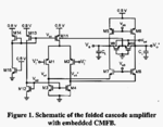
folded cascode amplifier.PNG


Here for the above circuit the following explaination is given:
Let us assume during the fabrication, the W/L ratio or the
threshold voltage of transistor MI2 is changed such that
the biasing voltage v b z is increased from its designed
value. This will result in corresponding increased current
in active load transistors (M3 and M4). Therefore, the
output voltage of the first stage, as well as the output
voltage of the second stage is lowered. These voltage
variations are-detected by the CMFB mechanisms and
the body voltage of M11 is reduced. This, in turn,
increases the tail current and causes the output voltages
{WO]+V, al-), and (Vo+, Vi)} to rise. This way the
feedback compensates the perturbations Of Vb2.

But I am really not able to understand how by output voltage values are getting lowered by increasing the load current in M3 and M4. Please help!
 

Hi
Consider a simple case. You have a node (say X) and I1 current is flowing into it and I2 current is flowing out of it. If I1=I2, net charge being dumped at node X is 0, and its potential will not change. If I1 >I2, positive charge is being dumped into the node and its potential will start rising.If I1<I2, negative charge is being dumped into node X and its potential will fall down.

In your case, when the load current in M3 and M4 increases, it is similar to the last case in the above example (I1<I2). In fact all cmfb circuits work on the similar principle.
 

What you are saying for the curent part is true but not able able to map the same thing for the circuit. Can you please be more elaborative and explain step by step with respect to the circuit. I'll really appreciate that.
 

Status
Not open for further replies.

Similar threads

Part and Inventory Search

Welcome to EDABoard.com

Sponsor

Back
Top