Continue to Site

Welcome to EDAboard.com

Welcome to our site! EDAboard.com is an international Electronics Discussion Forum focused on EDA software, circuits, schematics, books, theory, papers, asic, pld, 8051, DSP, Network, RF, Analog Design, PCB, Service Manuals... and a whole lot more! To participate you need to register. Registration is free. Click here to register now.

splitting DC bias logic question

yefj

Advanced Member level 4
Joined
Sep 12, 2019
Messages
1,199
Helped
1
Reputation
2
Reaction score
3
Trophy points
38
Activity points
7,238
Hello , I have an amplfier board of QPA2575 the DC feeding GND Is at metal_3_bot while the RF signal has ground at metal_2_mid.
The DC connector is HUGE as shown below,basicly i need to simultaniosly feed all 4 amplifiers.
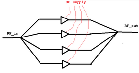
From looking at the data sheet i have this schemtics shown in the last photo.
How do i build a feeding network for such a complex connector so if will feed all 4 amplifiers shown in the schematics below.
Thanks.

1690700233015.png

1690701182426.png

1690698866921.png

1690699296503.png


1690699059072.png


1690699179854.png

1690701549163.png
 

Attachments

  • 1690701118261.png
    1690701118261.png
    8 KB · Views: 62
Hello, i have an amplifier QPA2575 which data sheet is attached.
As you can see below, i put the layout as i imagine it in the schematics.
for example if i what to simultaniosly power the drain_top(red arrow) DC input i dont know do to properly draw the trace from the main drain_top connector, to the sub (drain_top) at each amplifier.
Is there any intuition regarding how to simultaniosly power all four amplifiers?
Thanks.

1690864638437.png


1690865095436.png
 

Attachments

  • QPA2575 Data Sheet.pdf
    1.2 MB · Views: 66

LaTeX Commands Quick-Menu:

Part and Inventory Search

Welcome to EDABoard.com

Sponsor

Back
Top