yefj
Advanced Member level 4
Hello , I have tried to implement your advices and the result is shown below.
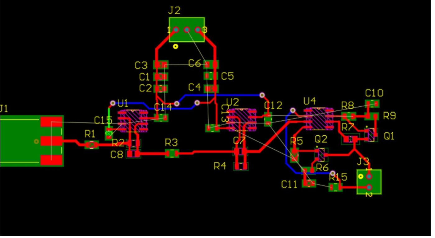
i have added 0.1uF bypass capacitors near each +`15V -15V trace of every IC.
Also decoupling capacitors where added near the 3 pin.
The problem is that i have many places where i need to supply the outputs of the 3 pin bias.
I know that i need to do polygon pour on both top and buttom layers which whould be GND .
I can route threw the buttom layers (using VIAs) i can route threw top layer.
what is the proper way to supply my IC's with +15 -15 GND?
I have tried to deliver +15 -15 using via's and buttom layers but it looks like a jungle.
If there is some more proper methodical way to do it?
PCB file is attached in the link.
 drive.google.com

i have added 0.1uF bypass capacitors near each +`15V -15V trace of every IC.
Also decoupling capacitors where added near the 3 pin.
The problem is that i have many places where i need to supply the outputs of the 3 pin bias.
I know that i need to do polygon pour on both top and buttom layers which whould be GND .
I can route threw the buttom layers (using VIAs) i can route threw top layer.
what is the proper way to supply my IC's with +15 -15 GND?
I have tried to deliver +15 -15 using via's and buttom layers but it looks like a jungle.
If there is some more proper methodical way to do it?
PCB file is attached in the link.
PCB1.PcbDoc
 drive.google.com