SDRookie
Junior Member level 2
Hi everyone.
I'm learning RFIC design now. I have a LNA works at 35GHz with SiGe. I designed a LNA that using common emitter with cascode method. In schematic simulation, the LNA is stable. However, the RLC extracted results shows the circuit is unstable.
I think one of the reason is that the wire connect between base and gnd is too long. Since it works at high frequency, the wire shows inductive. I searched online and everyone said the base (gate) to gnd layout need to be very "careful", but I don't know what should I do to make it a good gnd for base. I think in the layout, there has to be some distance between bondpad and base. Does the careful layout means the base has to be very very close to the ground bondpad?
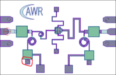
I searched some papers with layout picture. There is something I don't understand. I circled a small pad in the picture which is in attachment. The capacitor connected to a bondpad that is gnd. It also has that small pad connect to that capacitor. Is that pad also connect to the gnd? I'm very confused. why it could connect like that. If that small connect to ground, does it connect to exterior ground?
Please correct me if I'm wrong.
Thanks
I'm learning RFIC design now. I have a LNA works at 35GHz with SiGe. I designed a LNA that using common emitter with cascode method. In schematic simulation, the LNA is stable. However, the RLC extracted results shows the circuit is unstable.
I think one of the reason is that the wire connect between base and gnd is too long. Since it works at high frequency, the wire shows inductive. I searched online and everyone said the base (gate) to gnd layout need to be very "careful", but I don't know what should I do to make it a good gnd for base. I think in the layout, there has to be some distance between bondpad and base. Does the careful layout means the base has to be very very close to the ground bondpad?
I searched some papers with layout picture. There is something I don't understand. I circled a small pad in the picture which is in attachment. The capacitor connected to a bondpad that is gnd. It also has that small pad connect to that capacitor. Is that pad also connect to the gnd? I'm very confused. why it could connect like that. If that small connect to ground, does it connect to exterior ground?
Please correct me if I'm wrong.
Thanks