Continue to Site

Welcome to EDAboard.com

Welcome to our site! EDAboard.com is an international Electronics Discussion Forum focused on EDA software, circuits, schematics, books, theory, papers, asic, pld, 8051, DSP, Network, RF, Analog Design, PCB, Service Manuals... and a whole lot more! To participate you need to register. Registration is free. Click here to register now.

Cascode amplifier with different transistors

Young_Electronic_00

Newbie level 5
Joined
Sep 19, 2020
Messages
8
Helped
0
Reputation
0
Reaction score
0
Trophy points
1
Activity points
69
Hello all,

I found some schematic of cascode amplifier:
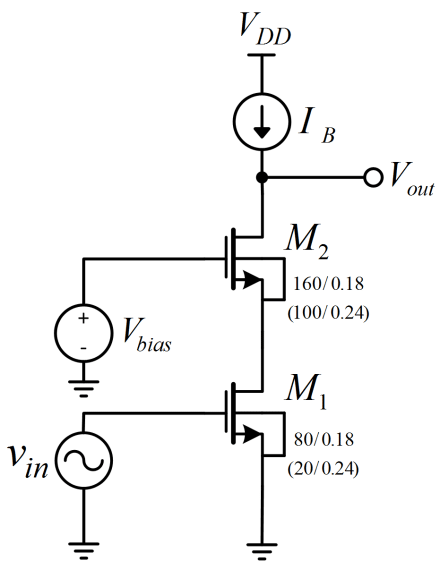
Cascode-Amplifier-All-transistor-sizes-W-L-are-in-m-Sizes-without-brackets-are-for-a.png


I'm just wondering why authors used transsistors having different parameters. Such configuration have some advantages in terms of operational banwdwidth or what ?

Best Regads,
Tom
 
Although you raised this issue in the Analog section, it certainly belongs to the Analog Integrated Circuit scope. That being the case, these are not exactly different discrete transistors, they are all on the same chip but just different dimensions. By the way, one of the main reasons for this is the proper biasing, given the voltage and current requirements given at each node of the circuit.
 
Hello Andre,

thank you for the response.

Although you raised this issue in the Analog section, it certainly belongs to the Analog Integrated Circuit scope.
You're absolutely right, so can we "shift" this topic to IC Analog sub-forum ?

By the way, one of the main reasons for this is the proper biasing, given the voltage and current requirements given at each node of the circuit.
Ok, but I don't get it... I mean, why - if this is case where biasing is most significant, why they haven't use two transistors with the same sizes ? I'm wondering how this solution works in higher frequencies (?).

Regards,
 
Because in analog IC design, you do not pick up identical transistors to adjust their biases, but rather to change their geometry to trim the dimensions of these transistors - thus making them different - in order to meet the given requirements defined by the above boundary conditions ( current "Ib", signal bias input "Vin", upper transistor bias "Vbias"). If you really want to know the effect on frequency of this "assymetry" review the gain expression or do a KCL analysis.
 
In many basic CMOS IC technologies you could not tie
the two FETs' bodies separately to their local source as
shown, because Psub! is global. Only a triple-well or
SOI flow (or discretes) will enable what's shown.

So given the inevitable body effect you might then size
the "guard" transistor up to make its Vgs(op) less of a
headroom-killer (maybe to the tune of half a volt?).
 

LaTeX Commands Quick-Menu:

Part and Inventory Search

Welcome to EDABoard.com

Sponsor

Back
Top