Continue to Site

Welcome to EDAboard.com

Welcome to our site! EDAboard.com is an international Electronics Discussion Forum focused on EDA software, circuits, schematics, books, theory, papers, asic, pld, 8051, DSP, Network, RF, Analog Design, PCB, Service Manuals... and a whole lot more! To participate you need to register. Registration is free. Click here to register now.

RF PCB Design - Need help with filter tuning and impedance matching

Status
Not open for further replies.

prusaga

Newbie level 3
Joined
Nov 2, 2016
Messages
4
Helped
0
Reputation
0
Reaction score
0
Trophy points
1
Activity points
41
Hello everyone,

I am new to PCB design. I am working on RF based PCB design with SMA antenna. I am working from a reference design whose filter design values are unclear. I have already tested a board and failed to make it work. This time I want to make sure that my component values and trace lengths are perfect.

I have installed ADS but confused as to what tools to use like harmonic balance or impedance matching tool etc. For PCB design I am using KiCAD.

Thank You.
 

You're newbie and I'm not very sure that you know how to use ADS.It's quite complicated package for novice users..
What type of filter you need ?? Perhaps I can help you..
 

What is the type of filter you want? What topology? What is the frequency? How can you expect to get everything right on this pass when the design values are not known?
 

Thanks for the help. I am working on board which has initially a balun and then a filter. Then we have a power amplifier and filter ending into a SMA. Some of the values of the components are not correct from the reference design I am working from. I am unsure of the trace lengths and unable to understand the blue filter towards the right of picture. Thank you again. filter and balun.PNG
 

I apologize for the missing information regarding the circuit. I have attached the RF part of the schematic.filter and balun.PNG It contains an IC SE2345L whose PA is being used for transmission. Some of the component values are incorrect as they were unclear in the reference design I'm working from. In the attached schematic the final series L and C is also not clear.

This part of the schematic I am planning to simulate in ADS with the component values and equivalent impedance for the traces and use it to tune the trace lengths and also the component values.
 

It's not clear which part of the circuit you are referring to. There's the transceiver balun and the SE2345 filter and impedance matching circuitry. You have marked a series LC circuit that isn't shown in the original reference design, so we can only guess about it's necessity.

The most serious problem is the SE2345 datasheet doesn't specify actual PA and LAN impedances, just states that they are "50 ohm matched", not saying if with or without additional LC components. You are able to model the PCB and LC component behavior but not the transceiver or SE2435 impedances in lack of exact data.

The usual procedure is to start from a reference design, measure the achieved matching and harmonic suppression and tune it empirically. Alternatively you might try to determine the port impedances of the involved components accurately and optimize the LC networks in a simulation. But due to the non-linear characteristic of transceiver and SE2435 PA, the actual matching results might be different. A final measurement is always required.

All-in-all, you either have the equipment and knowledge to perform the required measurement in operation or rely on the performance of published reference designs.
 

The reference design of circuit involving SE2435L which I am trying to implement is refe.PNG. As I had mentioned earlier the values are unclear.

I was referring to the red circled part. That part of the filter I am unable to understand.

Thank you for guiding and pointing out that the power amplifier of SE2435 cannot be modeled for the simulation. I guess I have to tune the components and trace empirically now.
 

The series circuit is tuned to about 2.2 GHz, either intended for harmonic suppression in Tx or to block interferences in Rx mode. I don't see it in the original Skyworks reference design.
 

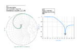
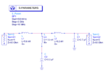
The circuit which has been marked in red seems to create a transmission zero on the transfer function of the matching circuit.
The response is follows and as you may see easily there is null @ 2.26GHz that is approximately 3rd harmonics ( rough estimation) of the carrier in order to limit the harmonic levels.

match_circuit.pngmatch_out.png
 
Status
Not open for further replies.

Part and Inventory Search

Welcome to EDABoard.com

Sponsor

Back
Top