Continue to Site

Welcome to EDAboard.com

Welcome to our site! EDAboard.com is an international Electronics Discussion Forum focused on EDA software, circuits, schematics, books, theory, papers, asic, pld, 8051, DSP, Network, RF, Analog Design, PCB, Service Manuals... and a whole lot more! To participate you need to register. Registration is free. Click here to register now.

Bilateral Impedance Matching Design

jadnounyah

Junior Member level 3
Joined
Aug 21, 2022
Messages
30
Helped
0
Reputation
0
Reaction score
0
Trophy points
6
Activity points
297
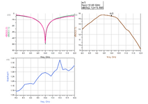
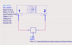
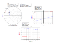
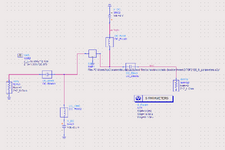
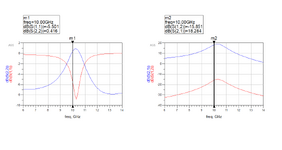
I used S11 and S22 as a first step in finding the simultaneous matching network, but I'm not sure where to go from here.

They outputted:
S11 @ 2.4GHz = 1.339+20.873j
S11 @ 2.4GHz = 18.634+12.409j

How do I go about the bilateral design from here, I really don't know how to get the matching done simultaneously. It's in ADS, any help even if you used different impedances
 
You have S11 and S22. All you have to do is to create a Matching Circuit for both Input and Output.
I guess how to design a Matching Circuit using with s-parameters.
 
You may need to reduce trace inductance too to achieve a better s21 with controlled impedances. Bilateral is just linear passive.
Distributed as ;
pH/mm * mm/pF = pH/pF= ohm^2 for s11,s22 = R + sX(f)

For 50 ohm if C 3pF/mm then L must be sqrt(50^2 * 3^2) = 150 pH/mm

So from your results you have too much L and not enough C which means thinner substrate to Gnd and wider traces.
 
Last edited:
If you're able to access to MatchCAD, I can post here calculation template. This template computes Simultaneously Matching Conditions and Associated Source and Load Reflection Values ( Gamma_S and Gamma_L )
Once you have obtained these values, Matching Circuits can be designed by using different techniques.
 

Attachments

  • Amplifier_Design.pdf
    395.3 KB · Views: 61
You have S11 and S22. All you have to do is to create a Matching Circuit for both Input and Output.
I guess how to design a Matching Circuit using with s-parameters.
I thought that was for unilateral matching? Doing the matching separately?
--- Updated ---

Here is a video on that exact topic using ADS:

I think you also need S21 and S12
Thanks a lot and I'm also reading Gonzalez's book on the design. Very helpful.
--- Updated ---

You may need to reduce trace inductance too to achieve a better s21 with controlled impedances. Bilateral is just linear passive.
Distributed as ;
pH/mm * mm/pF = pH/pF= ohm^2 for s11,s22 = R + sX(f)

For 50 ohm if C 3pF/mm then L must be sqrt(50^2 * 3^2) = 150 pH/mm

So from your results you have too much L and not enough C which means thinner substrate to Gnd and wider traces.
That was what I obtained after running simulation for Sparameters with biasing. How do I make it better?, I believe it's more like the intrinsic performance of the active device with that specific bias at 10 GHz.
--- Updated ---

If you're able to access to MatchCAD, I can post here calculation template. This template computes Simultaneously Matching Conditions and Associated Source and Load Reflection Values ( Gamma_S and Gamma_L )
Once you have obtained these values, Matching Circuits can be designed by using different techniques.
Oh alright, thanks alot . I don't think I have access to MathCAD though but I have obtained help from the video posted by @volker and it'll work directly in ADS too for the matching to be complete. I appreciate the help though.
 
Last edited:
I have verified my calculation using with BFU710F s_parameters @ 2.5V, 3.5mA @10GHz.As you can see , the results are almost same.
 

Attachments

  • Simultaneous Match Circuit.png
    Simultaneous Match Circuit.png
    534.9 KB · Views: 43
  • Simultaneous Match Circuit Output.png
    Simultaneous Match Circuit Output.png
    292.5 KB · Views: 48
  • Amplifier_Design.pdf
    395.2 KB · Views: 46
I have verified my calculation using with BFU710F s_parameters @ 2.5V, 3.5mA @10GHz.As you can see , the results are almost same.
You used the impedances obtained from your sparameter simulation to match. I am having trouble even with the unilateral match. I test the circuit using the s11* and s22* and the matching is still poor. So I don't even know how to perform the bilateral matching since my impedances are being funny with me. I have attached the pictures here. 1 and 2 are for the sparams simulation at 10 GHz and 3 and 4 are for the matching impedance testing and results respectively. The active device is the
TGF2120 GaAs pHEMT from Qorvo. Thank you.
 

Attachments

  • 1.png
    1.png
    36.5 KB · Views: 39
  • 2.png
    2.png
    52.6 KB · Views: 40
  • 3.png
    3.png
    51.2 KB · Views: 36
  • 4.png
    4.png
    27.1 KB · Views: 37
You used the impedances obtained from your sparameter simulation to match. I am having trouble even with the unilateral match. I test the circuit using the s11* and s22* and the matching is still poor. So I don't even know how to perform the bilateral matching since my impedances are being funny with me. I have attached the pictures here. 1 and 2 are for the sparams simulation at 10 GHz and 3 and 4 are for the matching impedance testing and results respectively. The active device is the
TGF2120 GaAs pHEMT from Qorvo. Thank you.
Because this Transistor is NOT stable @ 10Ghz.
Simultaneously Matching or in other words Bilateral Design (S12 is NOT Zero) can be possible only and only under these circumstances.
1708133828898.png

--- Updated ---

You bias s-parameter block ?? :rolleyes:
Dear friend,
s-parameters characterize a Circuit or System under Small Signal Conditions and Biasing has no effect at ALL.
You have to work on Basics of Microwave Engineering otherwise you cannot go forward in this way.
 

Attachments

  • TGF2120_10GHz.pdf
    403.3 KB · Views: 41
Last edited:
Because this Transistor is NOT stable @ 10Ghz.
Simultaneously Matching or in other words Bilateral Design (S12 is NOT Zero) can be possible only and only under these circumstances.
View attachment 188703
--- Updated ---

You bias s-parameter block ?? :rolleyes:
Dear friend,
s-parameters characterize a Circuit or System under Small Signal Conditions and Biasing has no effect at ALL.
You have to work on Basics of Microwave Engineering otherwise you cannot go forward in this way.
Oh alright then. Thanks a lot for the info, with the biasing, first time working with s2p files so it got a bit away from. I'll take your advice into serious consideration though. Thanks
 

LaTeX Commands Quick-Menu:

Similar threads

Part and Inventory Search

Welcome to EDABoard.com

Sponsor

Back
Top