Continue to Site

Welcome to EDAboard.com

Welcome to our site! EDAboard.com is an international Electronics Discussion Forum focused on EDA software, circuits, schematics, books, theory, papers, asic, pld, 8051, DSP, Network, RF, Analog Design, PCB, Service Manuals... and a whole lot more! To participate you need to register. Registration is free. Click here to register now.

Impedance matching seems unpredictable

Bobson2000

Junior Member level 2
Joined
Aug 23, 2023
Messages
20
Helped
0
Reputation
0
Reaction score
0
Trophy points
1
Activity points
292
Hi, i'm trying to do impedance matching of small piece of RF path.
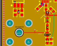
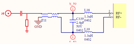
Target impedance is 50Ohm. I'm measuring it by VNA (calibrated, S11, Smith chart) connected port 1 to UFL connector (J4), from which path goes by 1nF capacitor (DC-block) to RF balun (impedance matching for mixer circut). First graphics shows layout, secons shows schematic. Traces (width, prepreg heigth) on PCB are calculated for about 50Ohm. Device is suppiled, and mixer circut is enabled when measerement is performed.
So, first measurement shows impedance 22,3,+3,7j. So i use will-kesley calculator which shows that i need just add series resistor about 27Ohm - so i added it, and impedance goes lower, not higher - i tried to add it after, befor, and instead of capacitor. In will-kesley calc first i set Z = 22 + 3.5j (meabe thats wrong way) and add series resistor. So i tried to make matching instinctively: i added a capacitor in series, and resistor i parallel as graphic shows, and after several tries, i found quite well values: 27pF, and 56Ohm, that gives impedance (measured) 49+20,35j.
1.Can somebody explain me whats going on? Its my almost first time with impedance matchning. Meabe these small piece of path have no siginifcant impact on whole RF path, meabe the shapes of pads vs. shapes of traces are make me this jokes, meabe i do measurement in wrong way? I tried the same method on another (different) piece of RF path, and impedance changes not according to what the calculator and manual calculations indicate.

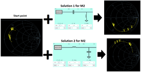
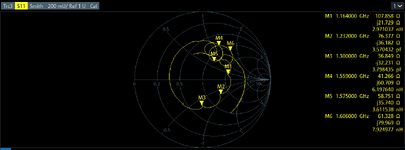
2.Second question is about impedance matching for two bands - third graphics - i want to move M5 and M2 points near middle of chart - is it possible by adding components?

I would be very grateful for any help.
Best regards
--- Updated ---

[EDIT] Meabe my method, or thinking is wrong, because substantially finaly the J4 (is just added for measurement, or input external signal) will be not used, and capacitor will be placed from L5 to balun (T7).
 

Attachments

  • Schemat.png
    Schemat.png
    375.4 KB · Views: 133
  • Bez tytułu1.png
    Bez tytułu1.png
    12.9 KB · Views: 128
  • Przechwytywanie.PNG
    Przechwytywanie.PNG
    34.5 KB · Views: 130
Last edited:
Traces are very thin. They will impact the Measured Impedances. Also VIAs are not sufficient, you have to place much more.
What exactly to match do you intend? What is Differential Impedance of the IC ?
Which Balun you have used ?? Are the s-parameters of Balun available ?? If yes, use them.
What is your overall bandwidth ??
Series resistance method is NOT used for this kind of matching purpose. How did you hear that ??
 
It's not even clear if the load (mixer) is suitable for impedance measurements respectively if the operation conditions are reasonable. Please give more details.
 
Hi, thansk for quick response.

BigBoss, and FvM:
In next revision it will have 3 vias per GND pad, i know that this one is not enaught. I haven't drawn the PCB, but I'm supposed to be developing it.
Balun is MABA-007159-000000, and mixer is LT5512. As i saw, the balun should have center-tap connected to GND, but used balun have no center-tap, so is selected wrong, but as i saw i can "repair" it by adding shunt chokes to GND from each RF input pin - i must do it - sure?. Impedance should be match to 50, or 75Ohm - thats information from datasheet, about impedance of RF input. Overal bandwith is GNSS, but in this circut i'm interested in about 1150-1300MHz. In balun datasheet the input impedance is shown on Smith chart, but how i can use it when PCB components (copper, components) impact on this impedance?

I do not hear about series resistance matching to this purpose, but each tutorial about impedance matching don't describe where i can't use it - so i concluded that there are no contraindications.

Sorry, is my almost first time with RF, i read about it, but as i see, many things need to ask about it.
 
Yes, LT5512 souces DC current to RF port and therefore needs symmetrical DC path for both inputs.

Datasheet has sufficient information to design impedance matching, I think.
 
There is an application circuit for 900MHz-2500MHz with a Center Tapped Transformer that is necessary for Inputs.
Why don't you use that ?
1692899813438.png

All you have to do to tune the Input Matching Circuit for 1150-1300MHz. It's not so difficult.
 
Hi, thanks.

Im not a designer of this design, i just launch the design. I follow the datasheet, and added two shunt 100nH (maximum i had under hand) coils and results are good (40+14j), i will try with another values. But when i will can, i wil try with center-tap balun. Volker: what is difference?

Whay can You say to my second (first post, and third graphics) question, about impedance matchning for two bands? In this place i have just SMA antenna socket and path goes to LNA input by AC-coupling capacitor.
 
But when i will can, i wil try with center-tap balun. Volker: what is difference?
If you use the transformer with additional separate L to ground, only a part of the current (the current into the transformer primary) is coupled to the secondary. Differential mode current will also flow through the shunt L, but there is no coupling to the output. This is equivalent to a transformer with weak coupling.

Remember that matching is only one of the goals, you also want to have low losses in your path. That's why some lossy configurations are not desirable, even if matching is ok.

Second question: Matching for multiple bands isn't trivial, especially if the location in Smith chart is far away like M2 and M5. But if you start using the configuration from the data sheet, it might be better than that. You might also have a look at software for matching network synthesis like OptenniLab, which can calculate multi-band matching.
 
Thanks for all.
As i see, that the 40+14j is maximum what can i achaive, but is about 6dB less reflected power in middle of band. For multiband i will try to use software.
 
Hi, i have almost succesed with LT5512 impedance matching, by shunt coils, because i have no tapped baluns.

Now i goes to first input section: SMA connector (for antenna) to first LNA (BGA824N6). Layout looks like on graphics below. Small shunt component near SMA is special protection diode with small capacitance. Path contain series coil and capacitor as datasheet sugest, but i get about -3 to -4,5dB reflected power on S11, so i replaced it coil and capacitor by 0R resistor, and try to do my own impedance matching: first for low band, and after that for upper band (as i found in some article about impedance matchin). So i removed it, measure impedance, and find two solutions (with will-kelsey calculator) for low band and i tried it, and gets results in graphics below. I don't understand why chart moves just according to first component (to capacitance, or to inductance). For shunt components i use GND wire marked by green line on layout graphics - meabe that's issue. I tried to reverse components order (just for curiousity), and thats not source of issue. Can somebody tell me what i'm doing, thinking, or have designed wrong? Meabe this mismatch occurs on SMA-copper path connection?
Copper path width are calculated for 50Ohm impedance. I se couple of videos, where somebeody takes some LNA, measure its input impedance by VNA, and just simply does impedance matching using will-kelsey calculator, and adding two components - for my its strongly working wrong :)
 

Attachments

  • Schemat.png
    Schemat.png
    402.8 KB · Views: 72
  • Solutions for M2.png
    Solutions for M2.png
    186.6 KB · Views: 66
For shunt components i use GND wire marked by green line on layout graphics
In your layout screenshot, I see a green wire connecting two ground pads (no signal path) !?

Other notes: the gap between SMA center pin pad and ground looks very narrow, is that really the correct gap size? I would expect that this creates a lot of parasitic shunt C at the SMA pad. The line that follows from SMA to components looks narrow, what is your effective substrate thickness to ground?

I don't understand your impedance matching measurements and circuits, what are we expected to see there?
 
Green wire is GND wire used as normal GND to whom i solder shunt components, because i have no GND polygon on top.

You are right - the center pin of SMA, as i simulated it as via in Saturn PCB Design, shows impedance about dozen ohms - that can be main source of problems, and it corresponds wih measured impedance - smaller than target 50Ohm. Prepreg thickness betwen red label and GND is 0.075mm, and trace width is 0.125mm - thats look OK.

Impedance matching measurement i showed on graphics is S11 Smith chart. I measure sweep 1-1.8GHz, but i'm looking just for frequencies marked as M2 (low band), and M5 (up band). Schematics on blue background are impedance matching circuts from Smith chart calculator - starting point is M2 from chart on left, and results are charts on right (not compatible with the calculator simulation).
 
Green wire is GND wire used as normal GND to whom i solder shunt components, because i have no GND polygon on top.
Oops! The wire itself will have some nH inductance to ground, which adds to your shunt impedance. That parasitic inductance is on the order of your 3.3nH SMD component value! Can you perhaps drill a hole for a shorter via to the backside?

The second solution that you calculated, with 5µF shunt C, is not possible at these frequencies. The self resonance of these large C values is too low, so that 5µF can't be implemented in real world at GHz frequencies.
 
Thanks for response.

I thought that this wire would disturb something, hence I mentioned it in the description. I thought about making a grommet, but the board has 10 layers, so in eventually I will dig into the first layer of copper GND and solder there.

This is 5pF, not 5uF - graphics compression ate part of the letter "p" :)

But tell me - it's possible to done impedance matching with this center SMA pad issue? Because it's difficult to correction - first solution i see is driling hole with proper diameter.
 
From curiosity, i added series resistor 39R to this path, and impedance moves closer to target, and i see about 5dB in low band, and 2dB in upper band power gain when I pass the signal from the generator to the SMA and measure it with a spectrum analyzer at the output of the LNA.
PS: sorry, i don't know how edit approved posts, so i wroted newer.
 
If you add a 39R resistor and impedance moves to the target, doesn't mean is a viable solution, due to the added loss.
For example a 10dB attenuator (not-terminated) has about 20dB return loss, and even better if is terminated. So it will improve a lot the matching, but will add 10dB loss to the circuit.

To have minimum loss from an impedance matching network have to use reactive components (L,C,TL, etc.)
 
Thanks.
In this case it's possible to done impedance matching without editing SMA center pad hole?
Of course using CL, and LC matching networks like in this article: https://www.antenna-theory.com/tutorial/smith/smithchartC.php

However, will the problem with the middle SMA pad effectively block attempts at impedance matching?
 
Ideally at high frequencies, the SMA connector RF model should be part of the simulation.
At frequencies lower than 2.4GHz, you may not use the model.
 
it's possible to done impedance matching without editing SMA center pad hole?
You should really fix the underlying issue = pad/gap dimensions.

One reminder regarding your matching efforts: you need to make sure that your S-parameters are measured at (or shifted to) the correct reference plane. You can test that by a short circuit on PCB, to make sure that this a short in your Smith chart indeed. If you have more than a few degrees of phase/length offset, the matching tools will not help you.
 

LaTeX Commands Quick-Menu:

Similar threads

Part and Inventory Search

Welcome to EDABoard.com

Sponsor

Back
Top