Continue to Site

Welcome to EDAboard.com

Welcome to our site! EDAboard.com is an international Electronics Discussion Forum focused on EDA software, circuits, schematics, books, theory, papers, asic, pld, 8051, DSP, Network, RF, Analog Design, PCB, Service Manuals... and a whole lot more! To participate you need to register. Registration is free. Click here to register now.

Inconsistent Impedance Matching Network of a SAW Filter

wonderfulnx

Newbie
Joined
Sep 10, 2023
Messages
5
Helped
0
Reputation
0
Reaction score
0
Trophy points
1
Location
Beijing, China
Activity points
92
Hi everyone, I've been trying to measure and use some EPCOS SAW Filters recently and found something strange with their impedance matching network. This strange point exists in many of their models and here I'm using the model "B39321B3741H110" as the example. I've attached the datasheet and the Impedance matching application note they provided below.

This SAW filter requires input and output matching at the same time. According to the datasheet, the impedance on both input and output ports (based on an ideal matching) is a 490 Ohm resistor in parallel with a 2.8pF capacitor (490 Ohm || 2.8 pF). In order to match a 50-ohm source/load, a simple LC matching is used as shown (center frequency 315Mhz).
屏幕截图 2023-09-11 222825.png

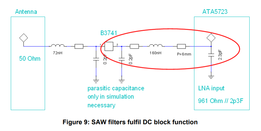
This matching network is consistent with the schematic given in application note 18 on page 11, where a 72nH inductor is used (not 74nH, probably considering the parasitic inductance of the PCB itself), as shown:
屏幕截图 2023-09-11 223401.png

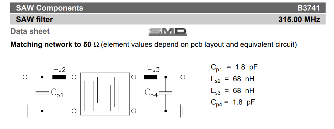
The 0.2pF capacitance is said to be considered only in simulation so I guess no need for them in actual PCB. But here comes the strange thing, the datasheet of this component clearly shows a matching network as this:
1694443126153.png

where the 0.2pF capacitor (close to the SAW) is gone and the series inductance continues to reduce to 68nH. And there is another capacitor in parallel that is close to the 50-ohm source. So why is there a 1.8pF capacitor here? Its purpose is not to substitute the 0.2pF one since they aren't in the same location. And it does not help the impedance matching here I think......
Also, How much is the typical value of parasitic inductance on a PCB, should the series inductance continue to reduce like this?

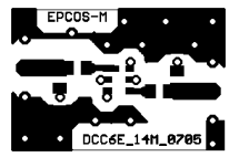
BTW, the suggested layout for this matching network is this:
屏幕截图 2023-09-11 224708.png
 

Attachments

  • B39321B3741H110.PDF
    118.2 KB · Views: 67
  • an18-matching-of-front-end-saw-filters-to-integrated-rke-receivers.pdf
    1.5 MB · Views: 106
I believe 490 Ohm || 2.8pF Input/Output Impedances are "Differential Impedances". You should consider them so and you have to divide these impedance by 2 then you can calculate "Single Ended Impedances-to-50 Ohm" matching components' values.

Single Ended Impedance is 245 Ohm || 5.6pF to "Virtual Ground". So you have to find a matching circuit for these values.
--- Updated ---

My comments above are not so correct. If a pin is grounded, the impedance will be same as in the datasheet.
The comment above might be used to match for diff-to-diff case.
 
Last edited:
Yeah, it's not a differential impedance, there is only one signal trace as the input and one as the output. I think the Cp1 and Cp4 capacitors here are still for compensating excess inductance or some other parasitic effect, but still can't get a compelling explanation.
 
Hi guys, just updating my progress with this matching thing and still having questions.

I'm actually using the B39921-B3300-H110 SAW component and have acquired the S-parameter files. The data sheet shows an input/output impedance of `360 || 1.0`(Ohm||pF) which is 68.0 - 141j (Ohm) at 916MHz. I matched it with the LC shown below and the result is perfect.
1.png
2.png

3.png

4.png


However, when working in a layout, another parallel capacitor is added before the inductor as shown in the official datasheet, having a value of about 2-3 pF. The guess is, that they are there to compensate for the parasitics induced by layout.
To explain this, I literally built a layout and simulated it in ADS, as shown:
5.png

But the result is bad, compared with the ideal matching case.
6.png


Now the thing is, whenever I remove the capacitor and increase the inductance value of the series L, the matching goes much better (changed the L to 22nH):
7.png


I see a similar discussion of this issue on this forum at https://www.edaboard.com/threads/saw-in-out-match-design.331642/. But I think there were misunderstandings of the S-parameter files back then, and my question on this problem is left unanswered: Why is there an extra parallel capacitor added in the official datasheet with their matching?
 
I've attached my layout ADS workspace below along with the S parameter files for B3300 (a narrow band one). Hope you guys will help me explain this thing.

Also, I'm in the process of fabricating the real evaluation board to see how it works. Now, I do accept that the simulation may be in many ways different from the real world. But as a student in research, I just want everything well explained. If I'm unable to at least explain this, I won't have the confidence to say that I do understand impedance matching....

The guess I have now is still that this is related to some parasitics. There is an explanation that the two inductors located on two sides of the SAW may have some magnetic coupling (since they are wire-wound inductors), which may eventually increase both of their inductance. Could that be the reason?
8.png


Anyway, I just want some good explanations of this...Maybe I'm too stubborn on this matter....🥴
--- Updated ---

I've attached my layout ADS workspace below along with the S parameter files for B3300 (a narrow band one). Hope you guys will help me explain this thing.
The attachments are here.
 

Attachments

  • SAW_Layout_wrk.zip
    362.9 KB · Views: 49
  • B3300s2p.zip
    118.7 KB · Views: 51
Last edited:
You're working on 315MHz SAW Filter Circuit but you supplied 915MHz SAW Filter s-parameters anyway.
OK, I have quickly worked a bit on this and find a reasonable results.
View attachment 1695679021932.png
View attachment 1695679046147.png
1695678489251.png


There is no difficulties at all. All you have to do is to draw a appropriate layout, find convenient matching components by "discrete optimization". It takes one hour or less.
Datasheets do have sometimes wrong informations and/or missing values, typo errors etc. Do not trust too much these datasheets.
 

Attachments

  • SAW_Working_wrk.rar
    4.2 MB · Views: 49
Thank you BigBoss! I found that the problem with my layout is the wrong configuration of the via bindings. Alongside my ADS layout and the one you kindly provided, I have also imported my board odb++ file to CST and conducted a simulation. The conclusion is unanimous, the simulation result we can get is indeed inconsistent with the datasheet. This means that the inconsistency is not brought by the layout. I think either it's some error in the datasheet, or it's indeed some parasitics that can't be simulated. I think I will wait for my evaluation board to check on this directly with VNA.
 

LaTeX Commands Quick-Menu:

Part and Inventory Search

Welcome to EDABoard.com

Sponsor

Back
Top