Continue to Site

Welcome to EDAboard.com

Welcome to our site! EDAboard.com is an international Electronics Discussion Forum focused on EDA software, circuits, schematics, books, theory, papers, asic, pld, 8051, DSP, Network, RF, Analog Design, PCB, Service Manuals... and a whole lot more! To participate you need to register. Registration is free. Click here to register now.

Impedance matching on Rf PCB

enemra

Junior Member level 1
Joined
Oct 19, 2011
Messages
17
Helped
0
Reputation
0
Reaction score
0
Trophy points
1,281
Activity points
1,422
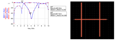
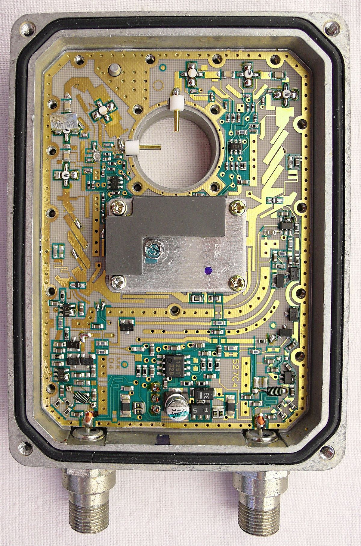
I have two questions in the image that I have attached. the image is of a power amplifier board.
  1. The output of the amplifier has irregular copper trace with different length until the output SMA, which I pointed as (1). Doesn't this impact the impedance of the trace?
  2. What is the use of two vertical traces before the output SMA, which I pointed as (2)?
enter image description here
Thank you
 

FvM

Super Moderator
Staff member
Advanced Member level 7
Joined
Jan 22, 2008
Messages
51,208
Helped
14,651
Reputation
29,580
Reaction score
13,795
Trophy points
1,393
Location
Bochum, Germany
Activity points
292,714
1. Stepped quarter wave transmission line for impedance matching
2. Transmission line stop filter for (probably 2nd) harmonic suppression
 

vfone

Advanced Member level 6
Joined
Oct 10, 2001
Messages
5,578
Helped
1,607
Reputation
3,219
Reaction score
1,213
Trophy points
1,393
Activity points
35,439
Should be a matching network, from the moment that in the datasheet is mentioned that the output impedance of BLF2425 is about 2.5ohms at 2450MHz.
 

enemra

Junior Member level 1
Joined
Oct 19, 2011
Messages
17
Helped
0
Reputation
0
Reaction score
0
Trophy points
1,281
Activity points
1,422
Thanks to all who answered. Amazing.... Learning on RF part is never ending :( Thanks for the heads up.
 

navet

Newbie
Newbie level 3
Joined
Feb 6, 2015
Messages
4
Helped
0
Reputation
0
Reaction score
1
Trophy points
1,281
Activity points
1,309
The section (1) is a matching network, his function is to present to the transistor some specific impedances (trade-off between efficiency and power output) in the band of interest.
The wide lines are near to the trans are low impedance, by stacking them together a transformer is created. Usualy this kind of network can be quarter wave sections / exponentiel tapper / or even Klopfeinstein taper (non linear step).

The section (2) is with no doubt a low-pass filter as an harmonic filter . The central freq of BLF2425 is 2.4GHz and according to the length of the stubs are tuned @ around 4.8GHz see attached a 10s quick EM simul.
 

Attachments

  • Sans titre.png
    Sans titre.png
    82.6 KB · Views: 20

LaTeX Commands Quick-Menu:

Part and Inventory Search

Welcome to EDABoard.com

Sponsor

Top