Continue to Site

Welcome to EDAboard.com

Welcome to our site! EDAboard.com is an international Electronics Discussion Forum focused on EDA software, circuits, schematics, books, theory, papers, asic, pld, 8051, DSP, Network, RF, Analog Design, PCB, Service Manuals... and a whole lot more! To participate you need to register. Registration is free. Click here to register now.

Question about opamp type?

Status
Not open for further replies.

samy555

Full Member level 4
Joined
May 11, 2010
Messages
207
Helped
0
Reputation
0
Reaction score
0
Trophy points
1,296
Location
Palestine
Activity points
2,963
Hi
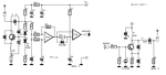
For the following circuit from:
https://electronics.stackexchange.com/questions/42923/what-do-i-need-for-a-basic-rf-circuit
fwySK.gif

I have 3 questions:
(1) Is LM311 is suitable fOr IC1 a & b?
(2) Why D1 & D2?
(3) What the function of the subcircuit consist of IC1b, R15 and D3?

thanks alot
 

1. the ICs have to amplify the data, so depends on your data rate - should be OK see :- **broken link removed**
2. D1 stabilised the DC operating conditions, D2 stabilises the squegging amplitude.
3. R15 +C10 are a peak detector so the comparator fires the output while the capacitor charges on positive peaks, R14 roughly charges C10 up at the same rate as its leakage current would discharge it, an example is shown in the data sheet.
Frank
 

2. D1 stabilised the DC operating conditions,
How and why?

D2 stabilises the squegging amplitude.
What is the squegging amplitude? I have not heard of it before!

3. R15 +C10 are a peak detector so the comparator fires the output while the capacitor charges on positive peaks, R14 roughly charges C10 up at the same rate as its leakage current would discharge it, an example is shown in the data sheet.
Is roughly charges = slowly charges?

Is that leakage current because C10 is electrolytic cap?

I understood that the signal output from IC1a charges C10 through R15 (when +ve peak) and at the same time battery charges C10 through R14 to compensate for the lost charge (leakage current),,, Is that true?

What is the role of the diode D3 here?

Thank you Frank
 

2. The voltage drop across D1 matches the volt drop across the Vbe of the transistor. This receiver is a super-regenerative type. Note the "super" is short for super sonic. the transistor actually oscillate at a supersonic frequency, which should be a lot higher then the data or channel bandwidth and a lot lower then the frequency its actually meant to use. The effect of this oscillation - called "squegging", is that the actual tuned circuits have positive feed back across them for part of the squegging cycle, this raises their Q and hence their sensitivity by a factor of 100 or so. In the old days the level was set manually and if mal-adjusted ,various howls and whistles would emerge from the radios loudspeaker, coupled with interferrence to adjacent radio users. :)
Frank
Can't get to your circuit now, link going to a different site?
 

Status
Not open for further replies.

Similar threads

Part and Inventory Search

Welcome to EDABoard.com

Sponsor

Back
Top