AtMega32
Junior Member level 3
I am designing a pure sinewave inverter, 220V, 50 Hz.
Here is the complete design,

without filter i simulate the whole circuit and tried to plot the current waveform by placing a current probe in RL Load (R = 5 Ohm, L = 16 mH).
I should be getting a sinusoidal current waveform but it is giving my arbitrary result. what might be the problem ?
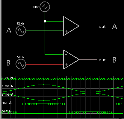
I have followed this article for PWM generation using Atmega16.
Switching Frequency 16 Khz.
Fundamental Frequency 50 Hz.
https://tahmidmc.blogspot.com/2013/02/sine-wave-generation-with-fast-pwm-mode_2525.html
An external crystal is being used for 16 Mhz clock frequency.
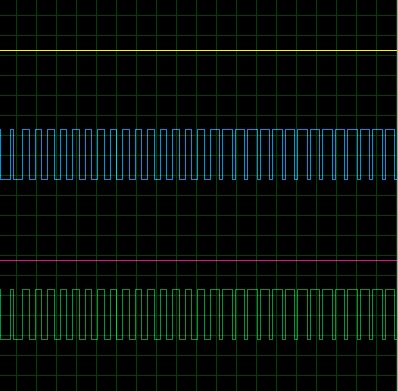
here is the configuration i have done .

Here is the PWM waveform


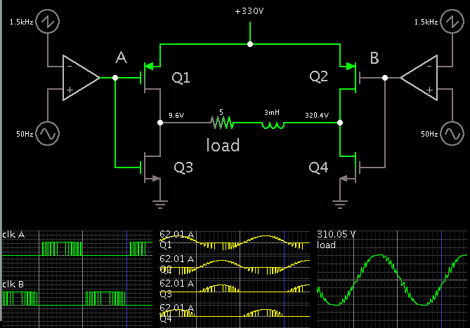
Instead of IR2110 i have used IR2112, as IR2110 is not available in Proteus. MOSFET Driver circuit is working fine, i have checked the voltage at gate and it is turning it ON/OFF.
MOSFETS are working good.
If i directly filter the PWM signal using RC filter i am getting a sinusoidal voltage waveform.
What might be the problem that i am not getting sinusoidal current waveform ????
If someone interested in debugging my circuit or just wants to run it in their Proteus please tell i will attach the design file.
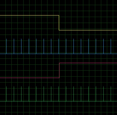
Here is what i am getting when simulate the circuit
Current waveform

Voltage Waveform

Any help will be appreciated
I wish tahmid is here to help me out, he is the best guy when it comes to share knowledge and helping out.
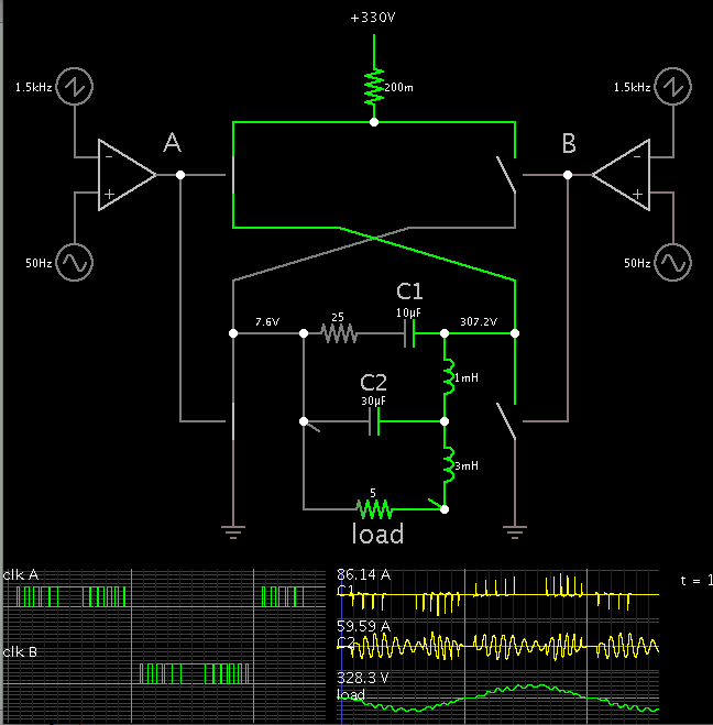
Here is the complete design,
without filter i simulate the whole circuit and tried to plot the current waveform by placing a current probe in RL Load (R = 5 Ohm, L = 16 mH).
I should be getting a sinusoidal current waveform but it is giving my arbitrary result. what might be the problem ?
I have followed this article for PWM generation using Atmega16.
Switching Frequency 16 Khz.
Fundamental Frequency 50 Hz.
https://tahmidmc.blogspot.com/2013/02/sine-wave-generation-with-fast-pwm-mode_2525.html
An external crystal is being used for 16 Mhz clock frequency.
here is the configuration i have done .
Here is the PWM waveform
Instead of IR2110 i have used IR2112, as IR2110 is not available in Proteus. MOSFET Driver circuit is working fine, i have checked the voltage at gate and it is turning it ON/OFF.
MOSFETS are working good.
If i directly filter the PWM signal using RC filter i am getting a sinusoidal voltage waveform.
What might be the problem that i am not getting sinusoidal current waveform ????
If someone interested in debugging my circuit or just wants to run it in their Proteus please tell i will attach the design file.
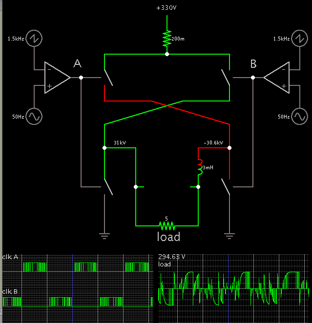
Here is what i am getting when simulate the circuit
Current waveform
Voltage Waveform
Any help will be appreciated
I wish tahmid is here to help me out, he is the best guy when it comes to share knowledge and helping out.