Continue to Site

Welcome to EDAboard.com

Welcome to our site! EDAboard.com is an international Electronics Discussion Forum focused on EDA software, circuits, schematics, books, theory, papers, asic, pld, 8051, DSP, Network, RF, Analog Design, PCB, Service Manuals... and a whole lot more! To participate you need to register. Registration is free. Click here to register now.

Poly cap missing problem

Status
Not open for further replies.

VLSI_Learner

Member level 2
Member level 2
Joined
Oct 26, 2012
Messages
51
Helped
0
Reputation
0
Reaction score
0
Trophy points
1,286
Visit site
Activity points
1,594
1. If there is no poly cap, then poly ends (up/down) will align with diffusion edges. Why it is not done? What problem it might create?
2. If poly is smaller than the diffusion (device) width, what problem it might cause?

For reference please see the picture.

1.jpg
 

1. If there is no poly cap, then poly ends (up/down) will align with diffusion edges. Why it is not done? What problem it might create?
The first mask is the active (TOX) definition mask. In order to compensate for possible displacement between this previous active and the following poly gate masking, there's a finite overlap of poly necessary (and stipulated by design rules), called poly cap.

S/D (NMOS and PMOS) formation by diffusion or implant is a self-aligned process, i.e. (additionally to the NMOS or PMOS mask) masked by the poly gate. The a.m. poly cap also considers a small under-diffusion or -scattering (which also decreases the effective channel length below the drawn length).

2. If poly is smaller than the diffusion (device) width, what problem it might cause?
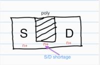
Obviously a (partly) continuous n+ or p+ region would be created, shorting S and D.
 

I can't get the idea of S/D shorting. Please explain.
- - - Updated - - -

So you mean that poly cap is only needed for poly and S/D alignment as it's a self aligned process? But the alignment occurs along the length, not along the width. So again can't get the idea properly.
 

I can't get the idea of S/D shorting. Please explain.
Hope I can make it clear with the help of this shorted nMOSFET:

So you mean that poly cap is only needed for poly and S/D alignment
Poly cap - also called poly extension or poly overhang - is needed against mis-alignment between active area (thin oxide definition) and poly, and the later following S/D implant.

... as it's a self aligned process? But the alignment occurs along the length, not along the width. So again can't get the idea properly.
I think you're mixing up two different alignment occurrences: self-alignment and (possible) mis-alignment. Both are concerned:

Right: self-alignment regarding the channel formation concerns the length of the channel. The poly cap, however, is necessary to avoid the situation shown in the image above: if there were a mis-alignment between the active area (thin oxide definition) mask and the poly mask (in the direction of the channel's width), without the poly extension an S/D shorting could occur.

Hope I could make this clear now. You might perhaps want to read the explanation given in , see Poly extension from diffusion on p. 32 (p. 38 of the PDF) .
 

Thank you. I understood your explanation. But there is a small thing that is bothering.
During fabrication first two diffusion layers are drawn, but they are placed some distance apart (channel). And on top of that spacing between two active areas poly (here short poly than the diffusion width) is deposited. So basically there should not be any short between S/D region. So I guess only the device width reduces.
 

I think you misunderstand the order and significance of the mask steps, sorry. I try to make this clear, leaving out the (many) intermediate steps, which aren't necessary for understanding the MOSFET formation process. Only valid for self-aligned gate processes:

1. Active Mask: Definition of the thin oxide (TOX) regions for all MOSFETs (NMOS & PMOS)
2. Poly Mask: Defines all poly gates (and poly capacitors) over TOX, poly gate extensions, poly connections and poly resistors over field oxide (FOX)
3. N+ S/D Mask: coincides but overlaps all TOX regions for NMOSFETs
4. P+ S/D Mask: coincides but overlaps all TOX regions for PMOSFETs

Below pls. find a process layout tutorial by Ken Martin which might help for understanding. See slides 9-12 for the a.m. self-aligning gate process. Slide 16 shows possible misalignment problems: View attachment 02_processing_layout.pdf
 

Well, my mistake. Poly is created first and then S/D region is created.
But is there only one mask for S and D region. And poly edge decides the channel-wise spacing between S/D region. Am I right?
 

Status
Not open for further replies.

Part and Inventory Search

Welcome to EDABoard.com

Sponsor

Back
Top