curious_kid
Newbie level 2
Hi All,
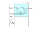
I am attaching a circuit diagram.
This circuit is basically trying to generate a double pulse for atspeed test vector generation. It could be for anything else, so don't worry about the functionality
The way it works is there is an asynchronous signal force_2_pulse, it is synchronized using a 2 flop synchronizer.
Whenever this signal comes, the pll clock is used to generate two high speed pulses for at-speed testing. This clock comes out as clock.
Sel 1 and Sel2 are also chip level pins and there selection determines whether the 2 pulses from pll output will go the logic ahead or normal slow speed clock
My question to you guys is
1. Could you please help me analyze what could be possible timing violations in this circuit? Like glitches, setup, hold violations.
Thanks a lot