sakibnaz
Full Member level 3
Hi there.
I am designing a Single Cell Li-Po Charger supporting 3A Charge current. I choose MP2617BGL-Z Charge Controller IC.

 www.monolithicpower.com
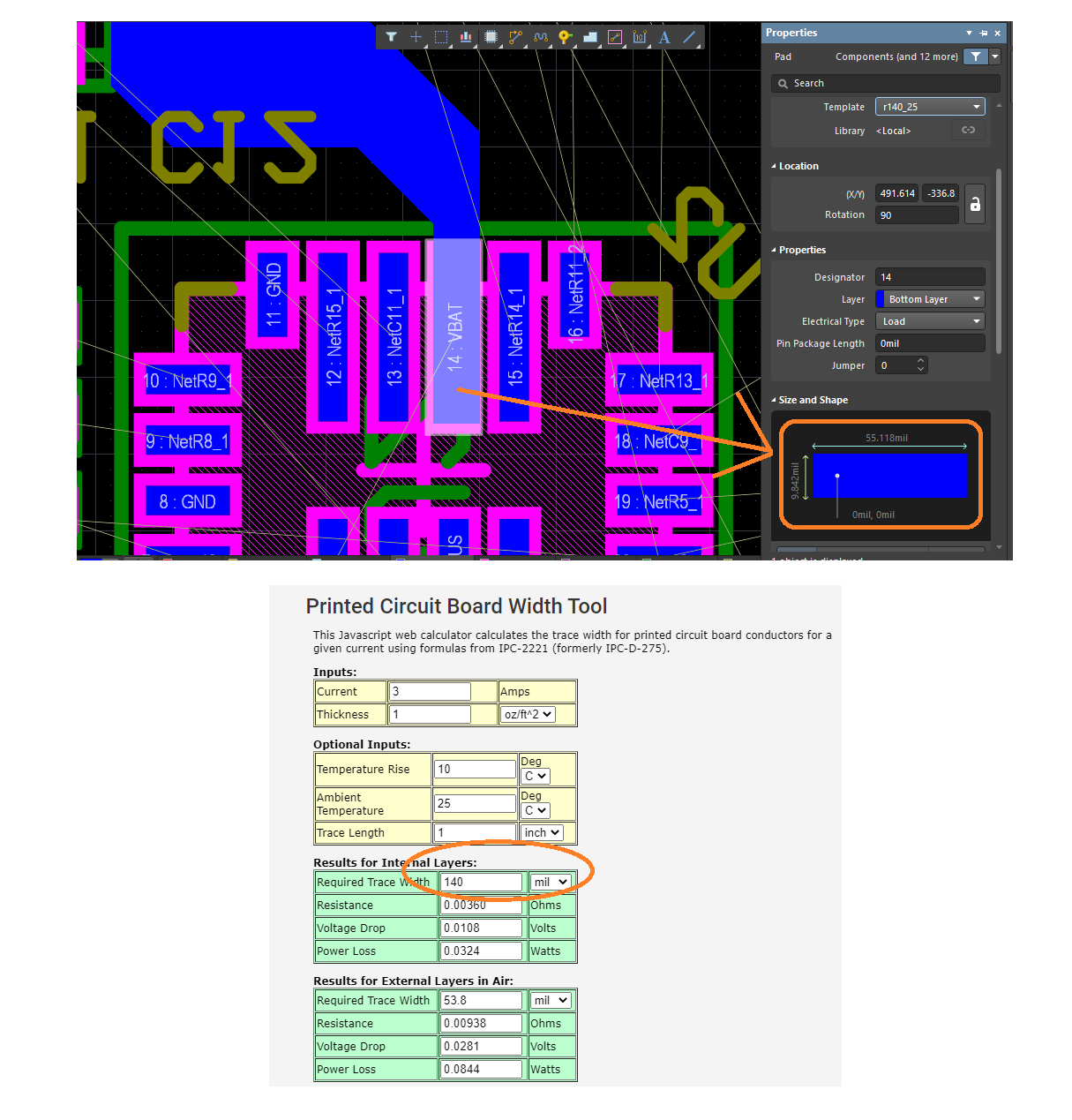
Now I have a ques about PCB Design mainly Tare Width. The PCB Pad size of the IC VBAT pin is around 55mil x 10mil. So my Trace min width will be less than 10mil. Then how can it carry 3A current?

According to https://www.4pcb.com/trace-width-calculator.html Width needs to be 140mil.
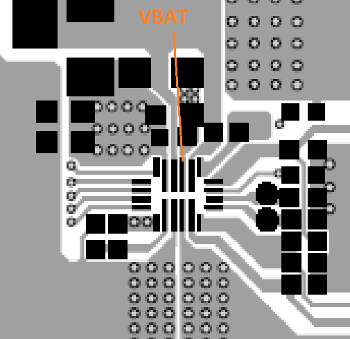
Also I checked the official Evaluation Kit design their min Trace will be less than 10mil as well close to the IC Pad.

Please advise how to do the design.
Thanks in advance.
Regards.
I am designing a Single Cell Li-Po Charger supporting 3A Charge current. I choose MP2617BGL-Z Charge Controller IC.

MP2617B
3A Switching Charger with NVDC Power Path Management For 4.2V Single Cell Li+ Battery
Now I have a ques about PCB Design mainly Tare Width. The PCB Pad size of the IC VBAT pin is around 55mil x 10mil. So my Trace min width will be less than 10mil. Then how can it carry 3A current?
According to https://www.4pcb.com/trace-width-calculator.html Width needs to be 140mil.
Also I checked the official Evaluation Kit design their min Trace will be less than 10mil as well close to the IC Pad.
Please advise how to do the design.
Thanks in advance.
Regards.