ranaya
Advanced Member level 4
Hi All, few elementary questions :
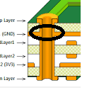
I am designing a multi layer PCB in Altium using the general 6 layer stackup format as shownn below :

1. Can we connect one of the internal signal layer pcb track (or internal plane) to a though-hole component pin (let's a pin of a 2.54 mm pitch pin header) without using vias to transfer the inner routing track to top or bottom layers ?
2. And how should I define drill pairs for the intended pcb design (the standard way)? i.e. Can we use top-to-bottom via and at the same time make it connected to the internal GND plane by tying via net to GND (in away it automatically connects GND plane) ? Atleast this is possible in Altium, but if it has to be connected to GND plane, shouln't we use tpp-Gnd or Gnd-Bottom vias ?
I am designing a multi layer PCB in Altium using the general 6 layer stackup format as shownn below :

1. Can we connect one of the internal signal layer pcb track (or internal plane) to a though-hole component pin (let's a pin of a 2.54 mm pitch pin header) without using vias to transfer the inner routing track to top or bottom layers ?
2. And how should I define drill pairs for the intended pcb design (the standard way)? i.e. Can we use top-to-bottom via and at the same time make it connected to the internal GND plane by tying via net to GND (in away it automatically connects GND plane) ? Atleast this is possible in Altium, but if it has to be connected to GND plane, shouln't we use tpp-Gnd or Gnd-Bottom vias ?
