Continue to Site

Welcome to EDAboard.com

Welcome to our site! EDAboard.com is an international Electronics Discussion Forum focused on EDA software, circuits, schematics, books, theory, papers, asic, pld, 8051, DSP, Network, RF, Analog Design, PCB, Service Manuals... and a whole lot more! To participate you need to register. Registration is free. Click here to register now.

positive and negative plane in pcb design software

engr_joni_ee

Advanced Member level 3
Joined
Nov 3, 2018
Messages
750
Helped
2
Reputation
4
Reaction score
4
Trophy points
18
Activity points
6,229
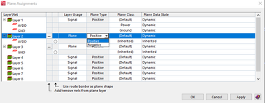
Hi, I am using mentor graphic tool. I search in the help which describe the positive and negative planes as:
  • Positive — Defines a positive plane.
  • Negative — Defines a negative plane. Changes the Plane Data State to "Batch".
I am not able to understand what are these positive and negative planes. It it the plane for positive voltages and negative voltages ? or it is positive for power supplies and ground for negative plane ?
 
Positive and negative refers to the way of generating the gerbet output. Positive plane draws copper features, negative the voids. Negative plane is actually a legacy from mechanical photo plotter age where it took hours to plot a large positive plane. Thus it was plotted negative and inverted photomechanically. All recent PCB tools are using positive gerber output for copper layers, only solder mask artwork is plotted negative.
 
You don't say WHICH Mentor tool, but I think this means whether you're displaying copper (positive) or absence of copper (negative). For example, solder mask layers are generally negative; the colored areas show where there's NO solder mask. Same for power planes, the copper areas are blank, the places with no copper are colored.
 
I think now I am getting the concept. By default if in the design tool, the plane are drawn as positive plane, means that the drawn shape is copper on the particular layer. But if we change in the setting that the planes to be drawn as negative then do we need to draw only those shapes where we don't need copper ?
 
It would help to know which Mentor tool you are using. Believe I never came across negative planes in Mentor Expedition. Guess you are rather working with Pads?
 
VX PCB Xpeditation has the option to define the plane as negative under plane assignment.
 

Attachments

  • Untitled 238.png
    Untitled 238.png
    22.2 KB · Views: 65
Read the full documentation. You find this comment in Expedition PCB Routing Solution Guide:
Avoid using negative planes for normal design work. Negative planes do not support the latest features for plane creation and editing (such as dynamic updating and hatching); they are available to maintain older legacy designs. With negative planes, batch DRC checks only for shorts between the plane boundary and other metal objects.
I think, this answers the question about usage of negative planes as far as normal designs are involved.
 
Negative planes are a piece of history, they were used because there was less data required when giving it to the board house. The fabricators engineer would convert it to a positive plane.

Modern tools do a lot more that require positive planes, they also give you a better ability to actually see where the plane covers and where it does not - you do however need a PC capable of displaying the whole board.

Today I would only use a positive plane.
 

LaTeX Commands Quick-Menu:

Part and Inventory Search

Welcome to EDABoard.com

Sponsor

Back
Top