Continue to Site

Welcome to EDAboard.com

Welcome to our site! EDAboard.com is an international Electronics Discussion Forum focused on EDA software, circuits, schematics, books, theory, papers, asic, pld, 8051, DSP, Network, RF, Analog Design, PCB, Service Manuals... and a whole lot more! To participate you need to register. Registration is free. Click here to register now.

PCB design and choosing number of layers

Status
Not open for further replies.

santu7885

Junior Member level 3
Joined
Sep 9, 2011
Messages
25
Helped
0
Reputation
0
Reaction score
0
Trophy points
1,281
Activity points
1,437
hi guys...

I m new to this forum n also new to Allegro (PCB design too). Let me know is that required to design a 4 layer board for design of DSP control board. If we can do with 2 layer board I think the number of via connections become more and cost of the board will increase. In 2 layer board we ned to take dynamic copper plane on two layers for ground and Vcc, that will add few more vias there(I m using only SMD components).

So please hlp me in choosing number of layers for my PCB??, How cost ll effect??and need some suggestions regarding routing....

Thanks in advance........
 

I would never use less than 4 layers for any digital based design, and havn't done for years, the difference in cost between 2 and 4 layers is not that much, and the benefits of having 4 layers with one a contigous ground plane far out wiegh the problems of trying to do the design on 2 layers and have so many compramises.
 

this is a very rough estimate as it varies with the complexity and specs

Layer count:
2 ---> 4 = 50 % difference
4 ---> 6 = 35-45 % difference
6 ---> 8 = 30-40 % difference
8 ---> 10 = very hard to estimate without Gerbers (window too big)

Copper platting:
1/2 oz ---> 1 oz = 2-5 % difference
1 oz ---> 2 oz = 10 % difference
2 oz ---> 3 oz = 15 % difference
 
I would never use less than 4 layers for any digital based design, and havn't done for years, the difference in cost between 2 and 4 layers is not that much, and the benefits of having 4 layers with one a contigous ground plane far out wiegh the problems of trying to do the design on 2 layers and have so many compramises.

Hi marce,

thnks for reply....

I already started design with 2 layers. I dont want to change the number of layers now. So I want to use a dynamic copper plane on bottom layer for ground. Is it helpful or not??...
One more Question is if there is any change in schmeatic(like if one of the schematic page changed totally).. How should we approach for back annotation, netlist and kepping the remaining components and routing as same...

thanks in advance...

---------- Post added at 09:04 ---------- Previous post was at 08:58 ----------

thanks lossemoose,

You have given valuable information.
I also want to know how much cost will add if use vias...??

thanks in advance...
 

Via cost isn't a problem of PCB price. Most PCB manufacturers don't charge them separately these days, possibly except for low-cost high volume production. Costs in terms of occupied area, signal integrity and reliablity is a different thing. Marce has clearly metioned some points against a two layer design. I don't know the application details, so I don't see a purpose in adding guesses about possible problems with your design.

Two layer implies, that a continuous ground can't be achieved, except for simple cases that have effectively single side wiring. The next best solution would be a tightly meshed ground. If it can be achieved neither, you should

- go for four layer, or
- do it as two layer somehow, pray for correct design operation, keep away from any EMC tests and don't complain at Edaboard about possible failure
 
thank you marce...
I completed my layout and I am doing artwork for each layer..
Now I am facing problem with silkscreen bottom...top bottom and silkscreen top are completed...
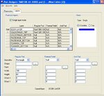
Please find the attached here... If possible give the solution....
components placed on bottom layer and it is SMD component...
this warning coming for all SMD pads on bottom layer...
thanks in advance...
 

Attachments

  • pad details.JPG
    pad details.JPG
    63.3 KB · Views: 92

I don't see, what silkscreen has to do with padstacks. If you didn't create the padstack yourself, I suspect some kind of confusion in the layer setup. If the problem is related to silkscreen, it should disappear, if you don't generate the silkscreen output. Does it?

I'm not familiar with Cadence PCB, however.

P.S.: Looking at the screenshot, it wonder what the table shows for bottom layer? Also, what's single layer mode? Are you sure that is what you want?
 

Status
Not open for further replies.

Part and Inventory Search

Welcome to EDABoard.com

Sponsor

Back
Top