Continue to Site

Welcome to EDAboard.com

Welcome to our site! EDAboard.com is an international Electronics Discussion Forum focused on EDA software, circuits, schematics, books, theory, papers, asic, pld, 8051, DSP, Network, RF, Analog Design, PCB, Service Manuals... and a whole lot more! To participate you need to register. Registration is free. Click here to register now.

[SOLVED] N-well(NW) and N-wel for high voltage(NWH) in smic18pf

Status
Not open for further replies.

b12345

Newbie level 6
Joined
Sep 30, 2011
Messages
11
Helped
0
Reputation
0
Reaction score
0
Trophy points
1,281
Activity points
1,381
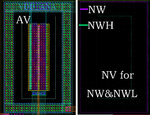
In a layout, I put both NW and NWH over a 5V PMOS, as follows
Could someone please tell me what it affects?THX
???-1.jpg
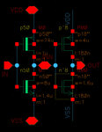
The circuit shown as follows, in the test, if the IN is high, the output is high, but if the INis low, the output turns to high from low afer 58ms, and there are signs that a large current about 1mA produced between VDD and VSS, thus we suppose the overlap of NW and NWH change the function of the PMOS, but we don't know how it works
schematic.jpg
 
Last edited:

hello,
Can you tell me why do you draw an NW in the NWH?
Although this is not disobey the design rule, but it is queer.
 

hello,
Can you tell me why do you draw an NW in the NWH?
Although this is not disobey the design rule, but it is queer.

Uhh...I made a mistake there...and the details are updated above

---------- Post added at 13:11 ---------- Previous post was at 12:59 ----------

Mm..hmm...
 
Last edited:

Re: N-well (NW) and N-well for high voltage (NWH) in smic18pf


I'm also using the smic18pf now. As his picture shown, it isn't disobey the design rule of the smic18pf. And i know the difference between the NW and NWH. So i just confused about the NW in the NWH. Although we don't draw the layout like this, if we do like this it is allowed. And the NWH is deeper than the NW, so the tolerance of the voltage isn't changed (still 5V). Am i right? By the way, the NWH is made before the NW from the mask ID.
 

Re: N-well (NW) and N-well for high voltage (NWH) in smic18pf


But, if there is a break down, where it is? Because VDD is high, so the operational environment of the PMOS is ensured. If the gate is low, source is high, body is high, how could my drain become low, it makes us confused.
Maybe the truth is more complicate than break down, we suppose, thanks for your reply :)

---------- Post added at 08:50 ---------- Previous post was at 08:40 ----------

Although it isn't disobey the design rule, but it is unreason indeed, and it may cause complex results that we cannot deduce it in a normal way, i think
 

Re: N-well (NW) and N-well for high voltage (NWH) in smic18pf

... the NWH is deeper than the NW, so the tolerance of the voltage isn't changed (still 5V). Am i right?
I don't think so: The breakdown voltage of the NW implant may already be close to 5V (ND ≈ 5e17). If another NWH implant is superimposed on the NW implant, both doping concentrations are added, hence the breakdown voltage will be even lower.

By the way, the NWH is made before the NW from the mask ID.
Of course. Deepest implants are made first.

---------- Post added at 14:47 ---------- Previous post was at 14:34 ----------

if there is a break down, where it is?
Between the superimposed NWH + NW and the substrate. With both implants superimposed you'll get into an impurity concentration range (5e17 .. 1e18) where the zener breakdown (as you mentioned above) already surmounts the avalanche breakdown (VB ≦ 5V).
 
  • Like
Reactions: b12345

    b12345

    Points: 2
    Helpful Answer Positive Rating
Hi erikl,

I know your meanings. The tolerance voltage of the PN junction has relation with the doping concentrations of the P and N. But i meant the doping concentrations of the P and N near by the depletion layer is still the NWH and P-sub. How about the tolerance voltage of this PN junction?
 

... i meant the doping concentrations of the P and N near by the depletion layer is still the NWH and P-sub. How about the tolerance voltage of this PN junction?

Hi windy,

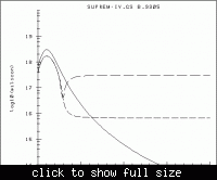
if you superimpose two or more implants (or diffusions) over each other, you'll have a larger impurity concentration than from a single implant -- at any depth (s. the plot below).

I.e. the breakdown voltage of the junction (in whatever depth the crossing of the implant and substrate impurity concentrations may occur) will always be lower than if there were only a single implant|diffusion.
 
Hi erikl,
Thank you for your reply, and i am sorry for replying your post so late.
 

Status
Not open for further replies.

Part and Inventory Search

Welcome to EDABoard.com

Sponsor

Back
Top