Continue to Site

Welcome to EDAboard.com

Welcome to our site! EDAboard.com is an international Electronics Discussion Forum focused on EDA software, circuits, schematics, books, theory, papers, asic, pld, 8051, DSP, Network, RF, Analog Design, PCB, Service Manuals... and a whole lot more! To participate you need to register. Registration is free. Click here to register now.

MOSCAP (MOS Capacitor)

Status
Not open for further replies.

syeda amna

Full Member level 4
Joined
Jun 1, 2010
Messages
222
Helped
24
Reputation
48
Reaction score
22
Trophy points
1,308
Location
Pakistan
Activity points
2,551
hi
What is MOSCAP?
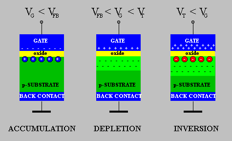
Please explain me accumulation depletion and inversion mode.
Any practical use of MOSCAP?
 

Its your lucky day, I just read this information last night!
A MOS CAP is basically a transistor without the DRAIN and SOURCE connections. This means that it has a GATE connection and a BODY seperated by a thin layer of insulating oxide, therefore, a CAP.

The operation of the moscap is illustrated by the image from wikipedia.

90_1305622605.gif
 

A capacitor is formed when two conducting layers are separated by a dielectric layer. In MOS, we have semiconductor (substrate) and Gate are separated by oxide layer. The value of MOS capacitor depends on the region of operation. See the link below:

**broken link removed**

**broken link removed**


MOS capacitor is exploited to store charge in DRAMs.

**broken link removed**
 
Last edited:

Thanks for your replies.I have some confusions in accumulation depletion and inversion modes. Why depletion region is wide at high frequency? What is the effect of low frequencies?
Please give some explanation.
 

Status
Not open for further replies.

Part and Inventory Search

Welcome to EDABoard.com

Sponsor

Back
Top